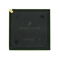
MPC561MZP56 Freescale, MPC561MZP56 Datasheet - Page 768

MPC561MZP56
Manufacturer Part Number
MPC561MZP56
Description
Manufacturer
Freescale
Datasheet
1.MPC561MZP56.pdf
(1420 pages)
Specifications of MPC561MZP56
Cpu Family
MPC56x
Device Core
PowerPC
Device Core Size
32b
Frequency (max)
56MHz
Interface Type
QSPI/SCI/SPI/UART
Total Internal Ram Size
32KB
# I/os (max)
56
Number Of Timers - General Purpose
22
Operating Supply Voltage (typ)
2.6/5V
Operating Supply Voltage (max)
2.7/5.25V
Operating Supply Voltage (min)
2.5/4.75V
On-chip Adc
2(32-chx10-bit)
Instruction Set Architecture
RISC
Operating Temp Range
-40C to 125C
Operating Temperature Classification
Automotive
Mounting
Surface Mount
Pin Count
388
Package Type
BGA
Program Memory Type
ROMLess
Program Memory Size
Not Required
Lead Free Status / RoHS Status
Not Compliant
Available stocks
Company
Part Number
Manufacturer
Quantity
Price
Company:
Part Number:
MPC561MZP56
Manufacturer:
Freescale Semiconductor
Quantity:
10 000
Company:
Part Number:
MPC561MZP56R2
Manufacturer:
Freescale Semiconductor
Quantity:
10 000
- Current page: 768 of 1420
- Download datasheet (11Mb)
Modular Input/Output Subsystem (MIOS14)
17.9.3.5.3
The output port bit operation is selected by leaving both channels disabled, (i.e., by writing to neither
register A nor B). The EDPOL bit alone controls the output value. The same result can be achieved by
keeping EDPOL at zero and using the FORCA and FORCB bits to obtain the desired output level.
17.9.3.6
OPWM mode is selected by setting MODE[0:3] to 1xxx. The MODE[1:3] bits allow some of the
comparator bits to be masked.
This mode allows pulse width modulated output waveforms to be generated, with eight selectable
frequencies. Frequencies are only relevant as such if the counter bus is driven by a counter as a time
reference. Both channels (A and B) are used to generate one PWM output signal on the MDASM signal.
Channel B is accessed via register B1. Register B2 is not accessible. Channels A and B define respectively
the leading and trailing edges of the PWM output pulse. The value in register B1 is transferred to register
B2 each time a match occurs on either channel A or B.
The value loaded in register A is compared with the value on the 16-bit counter bus each time the counter
bus is updated. When a match on A occurs, the FLAG line is activated and the output flip-flop is set. The
value loaded in register B2 is compared with the value on the 16-bit counter bus each time the counter bus
is updated. When a match occurs on B, the output flip-flop is reset.
17-36
Output signal
Mode selection; MODE0 = 1
Internal Register, not accessible to software
Register B1
Register B2
Register A
FLAG bit
Counter Bus
16-bit
Output Pulse Width Modulation (OPWM) Mode
Output Port Bit Operation
A FORCA or FORCB does not cause a transfer from B1 to B2.
Write to A
0x1000
0xxxxx
0xxxxx
0x0500
Figure 17-20. Single Shot Output Transition Example
F LAG reset
by software
MPC561/MPC563 Reference Manual, Rev. 1.2
0x1000
0x1000
0xxxxx
0xxxxx
A Event
Reoccurences of the timer count do
not trigger a response unless registers
A or B have been written again.
0x1100
0x1000
0xxxxx
0xxxxx
NOTE
Write to B
0x1000
0x1000
0xxxxx
0x1100
B Event
0x1000
0xxxxx
0x1100
0x1100
FLAG reset
by software
Freescale Semiconductor
0x1000
0xxxxx
0x1000
0x1100
Related parts for MPC561MZP56
Image
Part Number
Description
Manufacturer
Datasheet
Request
R

Part Number:
Description:
MPC5 1K0 5%
Manufacturer:
TE Connectivity
Datasheet:

Part Number:
Description:
MPC5 500R 5%
Manufacturer:
TE Connectivity
Datasheet:

Part Number:
Description:
MPC5 5K0 5%
Manufacturer:
Tyco Electronics
Datasheet:

Part Number:
Description:
MPC5 5R0 5%
Manufacturer:
Tyco Electronics
Datasheet:

Part Number:
Description:
MPC5 50K 5%
Manufacturer:
Tyco Electronics
Datasheet:

Part Number:
Description:
MPC5 1R0 5%
Manufacturer:
Tyco Electronics
Datasheet:

Part Number:
Description:
TOWER ELEVATOR BOARDS HARDWARE
Manufacturer:
Freescale Semiconductor
Datasheet:

Part Number:
Description:
TOWER SERIAL I/O HARDWARE
Manufacturer:
Freescale Semiconductor
Datasheet:

Part Number:
Description:
LCD MODULE FOR TWR SYSTEM
Manufacturer:
Freescale Semiconductor
Datasheet:

Part Number:
Description:
DAUGHTER LCD WVGA I.MX51
Manufacturer:
Freescale Semiconductor
Datasheet:

Part Number:
Description:
TOWER SYSTEM BOARD MPC5125
Manufacturer:
Freescale Semiconductor
Datasheet:


