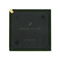
MPC561MZP56 Freescale, MPC561MZP56 Datasheet - Page 1048

MPC561MZP56
Manufacturer Part Number
MPC561MZP56
Description
Manufacturer
Freescale
Datasheet
1.MPC561MZP56.pdf
(1420 pages)
Specifications of MPC561MZP56
Cpu Family
MPC56x
Device Core
PowerPC
Device Core Size
32b
Frequency (max)
56MHz
Interface Type
QSPI/SCI/SPI/UART
Total Internal Ram Size
32KB
# I/os (max)
56
Number Of Timers - General Purpose
22
Operating Supply Voltage (typ)
2.6/5V
Operating Supply Voltage (max)
2.7/5.25V
Operating Supply Voltage (min)
2.5/4.75V
On-chip Adc
2(32-chx10-bit)
Instruction Set Architecture
RISC
Operating Temp Range
-40C to 125C
Operating Temperature Classification
Automotive
Mounting
Surface Mount
Pin Count
388
Package Type
BGA
Program Memory Type
ROMLess
Program Memory Size
Not Required
Lead Free Status / RoHS Status
Not Compliant
Available stocks
Company
Part Number
Manufacturer
Quantity
Price
Company:
Part Number:
MPC561MZP56
Manufacturer:
Freescale Semiconductor
Quantity:
10 000
Company:
Part Number:
MPC561MZP56R2
Manufacturer:
Freescale Semiconductor
Quantity:
10 000
- Current page: 1048 of 1420
- Download datasheet (11Mb)
READI Module
When the RCPU is in debug mode, program trace is not allowed. If program trace is enabled, a program
trace synchronization message is generated when debug mode exits.
When the RCPU is in debug mode, data trace and R/W access are allowed.
The flow chart in
of RCPU development access via READI are described below. Allowed modes are also summarized in
Table 24-8
24.14.2.1 Enabling RCPU Development Access Via READI Signals
Reset sequencing is done by the tool to initialize the READI signals and registers by asserting RSTI (the
device sends out the device ID message after the RSTI negation). System reset is held by the tool until the
READI module is reset and initialized with desired RCPU development access setting.
24.14.2.2 Entering Background Debug Mode (BDM) Via READI Signals
There are three ways to enter debug mode (provided debug mode has been enabled):
When entering debug mode following an exception/breakpoint, the RCPU signals VFLS[0:1] are equal to
0b11. This causes READI to send a BDM status message to the tool indicating that the RCPU has entered
debug mode and is now expecting instructions from the READI signals.
Debug mode enabling through READI and entering debug mode out of system reset is done by setting the
following bits in the DC register (DME=0b1, DOR=0b1) during system reset. Debug mode entry causes
RCPU to halt.
24.14.2.3 Non-Debug Mode Access of RCPU Development Access
The RCPU development access can be also be used while the RCPU is not halted (in debug mode). This
feature is used to send in breakpoints or synchronization events to the RCPU. Please refer to
“Development
Non-debug mode access of RCPU development can be achieved by configuring the READI module to take
control of RCPU development access during module configuration of the DC register (DME=0b0,
DOR=0bx).
24-80
1. Enter debug mode (halted state) out-of-system reset through READI module configuration. This is
2. Enter debug mode by downloading breakpoint instructions through RCPU development access
3. Enter debug mode if an exception or interrupt occurs.
displayed in
when in non-debug (running) mode.
of
Section 24.14.2.4, “RCPU Development Access Flow
The READI module will ignore any incoming DSDI data messages when
the module is not configured for RCPU development access.
Support” for further details.
Figure 24-83
Figure
24-84.
shows RCPU development access configuration via READI. The modes
MPC561/MPC563 Reference Manual, Rev. 1.2
NOTE
Diagram.”
Freescale Semiconductor
Chapter 23,
Related parts for MPC561MZP56
Image
Part Number
Description
Manufacturer
Datasheet
Request
R

Part Number:
Description:
MPC5 1K0 5%
Manufacturer:
TE Connectivity
Datasheet:

Part Number:
Description:
MPC5 500R 5%
Manufacturer:
TE Connectivity
Datasheet:

Part Number:
Description:
MPC5 5K0 5%
Manufacturer:
Tyco Electronics
Datasheet:

Part Number:
Description:
MPC5 5R0 5%
Manufacturer:
Tyco Electronics
Datasheet:

Part Number:
Description:
MPC5 50K 5%
Manufacturer:
Tyco Electronics
Datasheet:

Part Number:
Description:
MPC5 1R0 5%
Manufacturer:
Tyco Electronics
Datasheet:

Part Number:
Description:
TOWER ELEVATOR BOARDS HARDWARE
Manufacturer:
Freescale Semiconductor
Datasheet:

Part Number:
Description:
TOWER SERIAL I/O HARDWARE
Manufacturer:
Freescale Semiconductor
Datasheet:

Part Number:
Description:
LCD MODULE FOR TWR SYSTEM
Manufacturer:
Freescale Semiconductor
Datasheet:

Part Number:
Description:
DAUGHTER LCD WVGA I.MX51
Manufacturer:
Freescale Semiconductor
Datasheet:

Part Number:
Description:
TOWER SYSTEM BOARD MPC5125
Manufacturer:
Freescale Semiconductor
Datasheet:


