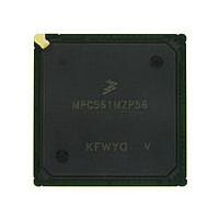
MPC561MZP56 Freescale, MPC561MZP56 Datasheet - Page 765

MPC561MZP56
Manufacturer Part Number
MPC561MZP56
Description
Manufacturer
Freescale
Datasheet
1.MPC561MZP56.pdf
(1420 pages)
Specifications of MPC561MZP56
Cpu Family
MPC56x
Device Core
PowerPC
Device Core Size
32b
Frequency (max)
56MHz
Interface Type
QSPI/SCI/SPI/UART
Total Internal Ram Size
32KB
# I/os (max)
56
Number Of Timers - General Purpose
22
Operating Supply Voltage (typ)
2.6/5V
Operating Supply Voltage (max)
2.7/5.25V
Operating Supply Voltage (min)
2.5/4.75V
On-chip Adc
2(32-chx10-bit)
Instruction Set Architecture
RISC
Operating Temp Range
-40C to 125C
Operating Temperature Classification
Automotive
Mounting
Surface Mount
Pin Count
388
Package Type
BGA
Program Memory Type
ROMLess
Program Memory Size
Not Required
Lead Free Status / RoHS Status
Not Compliant
Available stocks
Company
Part Number
Manufacturer
Quantity
Price
Company:
Part Number:
MPC561MZP56
Manufacturer:
Freescale Semiconductor
Quantity:
10 000
Company:
Part Number:
MPC561MZP56R2
Manufacturer:
Freescale Semiconductor
Quantity:
10 000
- Current page: 765 of 1420
- Download datasheet (11Mb)
17.9.3.5
Output compare mode (either OCA or OCB) is selected by setting MODE[0:3] to 0b010x. The MODE0
controls the activation criteria for the FLAG line, (i.e., when a compare occurs only on channel B or when
a compare occurs on either channel).
This mode allows the MDASM to perform four different output functions:
In this mode the leading and trailing edges of variable width output pulses are generated by calculated
output compare events occurring on channels A and B, respectively. OC mode may also be used to perform
a single output compare function, or may be used as an output port bit.
In this mode, channel B is accessed via register B2. A write to register B2 writes the same value to register
B1 even though the contents of B1 are not used in this mode. Both channels work together to generate one
‘single shot’ output pulse signal. Channel A defines the leading edge of the output pulse, while channel B
defines the trailing edge of the pulse. FLAG line activation can be done when a match occurs on channel
B only or when a compare occurs on either channel (as defined by the MODE0 in the MDASMSCR
register).
When this mode is first selected, (i.e., coming from disable mode, both comparators are disabled). Each
comparator is enabled by writing to its data register; it remains enabled until the next successful
comparison is made on that channel, whereupon it is disabled. The values stored in registers A and B are
compared with the count value on the selected 16-bit counter bus when their corresponding comparators
are enabled.
Freescale Semiconductor
•
•
•
•
Counter Bus
Mode selection; EDPOL = 0 (Channel A capture on rising edge)
Input signal
Internal Register, not accessible to software
Register B1
16-bit
Register B2
Register A
FLAG bit
(Ignored)
Single-shot output pulse (two edges), with FLAG line activated on the second edge
Single-shot output pulse (two edges), with FLAG line activated on both edges
Single-shot output transition (one edge)
Output port signal, with output compare function disabled
Output Compare (OCB and OCAB) Modes
0x0500
0xxxxx
0xxxxx
0xxxxx
Edge Trigger
Figure 17-18. MDASM Input Capture Example
Flag set
Rising
0x1000
MPC561/MPC563 Reference Manual, Rev. 1.2
0x1000
0x1000
0xxxxx
FLAG reset
by software
0x1000
0x1100
0x1000
0xxxxx
Edge Trigger
0x1400
0x1400
0x1000
Flag set
0x1400
Rising
FLAG reset
by software
Modular Input/Output Subsystem (MIOS14)
0x1400
0x1400
0x1000
0x1525
Flag set
Edge Trigger
0x16A0
0x16A0
0x1400
FLAG reset
by software
Rising
0x16A0
17-33
Related parts for MPC561MZP56
Image
Part Number
Description
Manufacturer
Datasheet
Request
R

Part Number:
Description:
MPC5 1K0 5%
Manufacturer:
TE Connectivity
Datasheet:

Part Number:
Description:
MPC5 500R 5%
Manufacturer:
TE Connectivity
Datasheet:

Part Number:
Description:
MPC5 5K0 5%
Manufacturer:
Tyco Electronics
Datasheet:

Part Number:
Description:
MPC5 5R0 5%
Manufacturer:
Tyco Electronics
Datasheet:

Part Number:
Description:
MPC5 50K 5%
Manufacturer:
Tyco Electronics
Datasheet:

Part Number:
Description:
MPC5 1R0 5%
Manufacturer:
Tyco Electronics
Datasheet:

Part Number:
Description:
TOWER ELEVATOR BOARDS HARDWARE
Manufacturer:
Freescale Semiconductor
Datasheet:

Part Number:
Description:
TOWER SERIAL I/O HARDWARE
Manufacturer:
Freescale Semiconductor
Datasheet:

Part Number:
Description:
LCD MODULE FOR TWR SYSTEM
Manufacturer:
Freescale Semiconductor
Datasheet:

Part Number:
Description:
DAUGHTER LCD WVGA I.MX51
Manufacturer:
Freescale Semiconductor
Datasheet:

Part Number:
Description:
TOWER SYSTEM BOARD MPC5125
Manufacturer:
Freescale Semiconductor
Datasheet:


