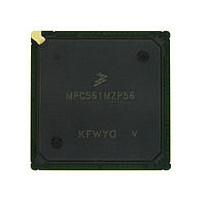
MPC561MZP56 Freescale, MPC561MZP56 Datasheet - Page 869

MPC561MZP56
Manufacturer Part Number
MPC561MZP56
Description
Manufacturer
Freescale
Datasheet
1.MPC561MZP56.pdf
(1420 pages)
Specifications of MPC561MZP56
Cpu Family
MPC56x
Device Core
PowerPC
Device Core Size
32b
Frequency (max)
56MHz
Interface Type
QSPI/SCI/SPI/UART
Total Internal Ram Size
32KB
# I/os (max)
56
Number Of Timers - General Purpose
22
Operating Supply Voltage (typ)
2.6/5V
Operating Supply Voltage (max)
2.7/5.25V
Operating Supply Voltage (min)
2.5/4.75V
On-chip Adc
2(32-chx10-bit)
Instruction Set Architecture
RISC
Operating Temp Range
-40C to 125C
Operating Temperature Classification
Automotive
Mounting
Surface Mount
Pin Count
388
Package Type
BGA
Program Memory Type
ROMLess
Program Memory Size
Not Required
Lead Free Status / RoHS Status
Not Compliant
Available stocks
Company
Part Number
Manufacturer
Quantity
Price
Company:
Part Number:
MPC561MZP56
Manufacturer:
Freescale Semiconductor
Quantity:
10 000
Company:
Part Number:
MPC561MZP56R2
Manufacturer:
Freescale Semiconductor
Quantity:
10 000
- Current page: 869 of 1420
- Download datasheet (11Mb)
Freescale Semiconductor
Bits
8:15
6:7
5
CENSOR Censor accesses. The CENSOR[0:1] bits are implemented using non-volatile register bits or CAM
ACCESS
Name
SUPV
Enable uncensored access. A censored access to the UC3F EEPROM is any access where the
device is in the censored mode.
The default reset state is ACCESS is a 0 so that FIC and CENSOR[0:1] control the state of
censorship to the UC3F EEPROM array. All accesses to the UC3F EEPROM array is allowed if
ACCESS = 1.
ACCESS can be read whenever the registers are enabled. ACCESS provides a method to bypass
the UC3F EEPROM module censorship.
0 Censored - UC3F array access allowed only if the censorship state is no censorship
1 Allows all UC3F array access
cells. The reset state of CENSOR[0:1] is user defined by the contents stored in the NVM register
bits.
CENSOR is not writable but the NVM register’s data can be set or cleared to the desired reset
state. Reading CENSOR while setting or clearing with the high voltage applied (CSC = 1 and HVS
= 1) will return 0’s.
00 cleared censorship, UC3F array access allowed only if device is in uncensored mode
01 no censorship, all UC3F array accesses allowed
10 no censorship, all UC3F array accesses allowed
11 information censorship, UC3F array access allowed only if device is in uncensored mode
Supervisor space. The SUPV bits are used to assign supervisor space restrictions for each block
of the UC3F array. The index for the SUPV bit field is used to determine block assignment. For
example, SUPV[0] is used for the supervisor space assignment of array block 0, while SUPV[4] is
used for array block 4 Supervisor space assignment.
Array block M is mapped into supervisor address space when SUPV[M] = 1, and only supervisor
accesses are allowed to array block M. If SUPV[M] = 0, then array block M is mapped into
unrestricted address space which allows both supervisor and user accesses to array block M.
The SUPV bits are not actually used in the UC3F EEPROM module but are used by the BIU to
determine access restrictions to UC3F array on a blockwise basis. The block addresses are
decoded in the BIU to determine which array block is selected, and the selected block’s SUPV bit
is compared with the address space attributes to determine validity of an array access.
When the small block function is enabled, the enabled small block portion of an array block is not
controlled by the SUPV bit corresponding to the array block containing that small block. This
particular small block is controlled by the appropriate SBSUPV bit while the remainder of that array
block is controlled by its SUPV bit.
0 array block M is placed in unrestricted address space
1 array block M is placed in supervisor address space
Table 21-3. UC3FMCR Bit Descriptions (continued)
MPC561/MPC563 Reference Manual, Rev. 1.2
Description
CDR3 Flash (UC3F) EEPROM
21-7
Related parts for MPC561MZP56
Image
Part Number
Description
Manufacturer
Datasheet
Request
R

Part Number:
Description:
MPC5 1K0 5%
Manufacturer:
TE Connectivity
Datasheet:

Part Number:
Description:
MPC5 500R 5%
Manufacturer:
TE Connectivity
Datasheet:

Part Number:
Description:
MPC5 5K0 5%
Manufacturer:
Tyco Electronics
Datasheet:

Part Number:
Description:
MPC5 5R0 5%
Manufacturer:
Tyco Electronics
Datasheet:

Part Number:
Description:
MPC5 50K 5%
Manufacturer:
Tyco Electronics
Datasheet:

Part Number:
Description:
MPC5 1R0 5%
Manufacturer:
Tyco Electronics
Datasheet:

Part Number:
Description:
TOWER ELEVATOR BOARDS HARDWARE
Manufacturer:
Freescale Semiconductor
Datasheet:

Part Number:
Description:
TOWER SERIAL I/O HARDWARE
Manufacturer:
Freescale Semiconductor
Datasheet:

Part Number:
Description:
LCD MODULE FOR TWR SYSTEM
Manufacturer:
Freescale Semiconductor
Datasheet:

Part Number:
Description:
DAUGHTER LCD WVGA I.MX51
Manufacturer:
Freescale Semiconductor
Datasheet:

Part Number:
Description:
TOWER SYSTEM BOARD MPC5125
Manufacturer:
Freescale Semiconductor
Datasheet:


