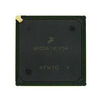
MPC561MZP56 Freescale, MPC561MZP56 Datasheet - Page 715

MPC561MZP56
Manufacturer Part Number
MPC561MZP56
Description
Manufacturer
Freescale
Datasheet
1.MPC561MZP56.pdf
(1420 pages)
Specifications of MPC561MZP56
Cpu Family
MPC56x
Device Core
PowerPC
Device Core Size
32b
Frequency (max)
56MHz
Interface Type
QSPI/SCI/SPI/UART
Total Internal Ram Size
32KB
# I/os (max)
56
Number Of Timers - General Purpose
22
Operating Supply Voltage (typ)
2.6/5V
Operating Supply Voltage (max)
2.7/5.25V
Operating Supply Voltage (min)
2.5/4.75V
On-chip Adc
2(32-chx10-bit)
Instruction Set Architecture
RISC
Operating Temp Range
-40C to 125C
Operating Temperature Classification
Automotive
Mounting
Surface Mount
Pin Count
388
Package Type
BGA
Program Memory Type
ROMLess
Program Memory Size
Not Required
Lead Free Status / RoHS Status
Not Compliant
Available stocks
Company
Part Number
Manufacturer
Quantity
Price
Company:
Part Number:
MPC561MZP56
Manufacturer:
Freescale Semiconductor
Quantity:
10 000
Company:
Part Number:
MPC561MZP56R2
Manufacturer:
Freescale Semiconductor
Quantity:
10 000
- Current page: 715 of 1420
- Download datasheet (11Mb)
16.7
Table 16-10
represents “A”, “B” or “C” for the TouCAN_A, TouCAN_B, or TouCAN_C module, respectively. Refer
to
The column labeled “Access” indicates the privilege level at which the CPU must be operating to access
the register. A designation of “S” indicates that supervisor mode is required. A designation of “S/U”
indicates that the register can be programmed for either supervisor mode access or unrestricted access.
The address space for each TouCAN module is split, with 128 bytes starting at the base address, and an
extra 256 bytes starting at the base address +128. The upper 256 are fully used for the message buffer
structures. Of the lower 128 bytes, some are not used. Registers with bits marked as “reserved” should
always be written as logic 0.
Typically, the TouCAN control registers are programmed during system initialization, before the TouCAN
becomes synchronized with the CAN bus. The configuration registers can be changed after
synchronization by halting the TouCAN module. This is done by setting the HALT bit in the TouCAN
module configuration register (CANMCR). The TouCAN responds by asserting CANMCR[NOTRDY].
Additionally, the control registers can be modified while the MCU is in background debug mode.
Freescale Semiconductor
Figure 1-4
Access
S
S
Programming Model
ILBS [1:0]
IMB3 CLOCK
IMB3 IRQ [7:0]
shows the TouCAN address map. The lowercase “x” appended to each register name
to locate each TouCAN module in the MPC561/MPC563 address map.
The TouCAN has no hard-wired protection against invalid bit/field
programming within its registers. Specifically, no protection is provided if
the programming does not meet CAN protocol requirements.
0x30 7080(A)
0x30 7480(B)
0x30 7880(C)
0x30 7082(A)
0x30 7482(B)
0x30 7882(C)
Address
Figure 16-7. Interrupt Levels on IRQ with ILBS
00
MPC561/MPC563 Reference Manual, Rev. 1.2
Table 16-10. TouCAN Register Map
01
IRQ
7:0
MSB
0
10
IRQ
15:8
NOTE
TouCAN Module Configuration Register (CANMCR_x)
23:16
11
IRQ
See
TouCAN Test Register (CANTCR_x)
31:24
Table 16-11
00
IRQ
01
IRQ
7:0
for bit descriptions.
.
10
CAN 2.0B Controller Module
11
LSB
16-21
15
Related parts for MPC561MZP56
Image
Part Number
Description
Manufacturer
Datasheet
Request
R

Part Number:
Description:
MPC5 1K0 5%
Manufacturer:
TE Connectivity
Datasheet:

Part Number:
Description:
MPC5 500R 5%
Manufacturer:
TE Connectivity
Datasheet:

Part Number:
Description:
MPC5 5K0 5%
Manufacturer:
Tyco Electronics
Datasheet:

Part Number:
Description:
MPC5 5R0 5%
Manufacturer:
Tyco Electronics
Datasheet:

Part Number:
Description:
MPC5 50K 5%
Manufacturer:
Tyco Electronics
Datasheet:

Part Number:
Description:
MPC5 1R0 5%
Manufacturer:
Tyco Electronics
Datasheet:

Part Number:
Description:
TOWER ELEVATOR BOARDS HARDWARE
Manufacturer:
Freescale Semiconductor
Datasheet:

Part Number:
Description:
TOWER SERIAL I/O HARDWARE
Manufacturer:
Freescale Semiconductor
Datasheet:

Part Number:
Description:
LCD MODULE FOR TWR SYSTEM
Manufacturer:
Freescale Semiconductor
Datasheet:

Part Number:
Description:
DAUGHTER LCD WVGA I.MX51
Manufacturer:
Freescale Semiconductor
Datasheet:

Part Number:
Description:
TOWER SYSTEM BOARD MPC5125
Manufacturer:
Freescale Semiconductor
Datasheet:


