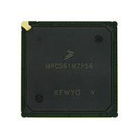
MPC561MZP56 Freescale, MPC561MZP56 Datasheet - Page 540

MPC561MZP56
Manufacturer Part Number
MPC561MZP56
Description
Manufacturer
Freescale
Datasheet
1.MPC561MZP56.pdf
(1420 pages)
Specifications of MPC561MZP56
Cpu Family
MPC56x
Device Core
PowerPC
Device Core Size
32b
Frequency (max)
56MHz
Interface Type
QSPI/SCI/SPI/UART
Total Internal Ram Size
32KB
# I/os (max)
56
Number Of Timers - General Purpose
22
Operating Supply Voltage (typ)
2.6/5V
Operating Supply Voltage (max)
2.7/5.25V
Operating Supply Voltage (min)
2.5/4.75V
On-chip Adc
2(32-chx10-bit)
Instruction Set Architecture
RISC
Operating Temp Range
-40C to 125C
Operating Temperature Classification
Automotive
Mounting
Surface Mount
Pin Count
388
Package Type
BGA
Program Memory Type
ROMLess
Program Memory Size
Not Required
Lead Free Status / RoHS Status
Not Compliant
Available stocks
Company
Part Number
Manufacturer
Quantity
Price
Company:
Part Number:
MPC561MZP56
Manufacturer:
Freescale Semiconductor
Quantity:
10 000
Company:
Part Number:
MPC561MZP56R2
Manufacturer:
Freescale Semiconductor
Quantity:
10 000
- Current page: 540 of 1420
- Download datasheet (11Mb)
QADC64E Legacy Mode Operation
In addition to internal junction leakage, external leakage (e.g., if external clamping diodes are used) and
charge sharing effects with internal capacitors also contribute to the total leakage current.
illustrates the effect of different levels of total leakage on accuracy for different values of source
impedance. The error is listed in terms of 10-bit counts.
13.7.5.4
Positive or negative stress refers to conditions which exceed nominally defined operating limits. Examples
include applying a voltage exceeding the normal limit on an input (for example, voltages outside of the
suggested supply/reference ranges) or causing currents into or out of the signal which exceed normal
limits. QADC64E specific considerations are voltages greater than V
an analog input which cause excessive currents into or out of the input. Refer to
Characteristics,” to for more information on exact magnitudes.
Either stress condition can potentially disrupt conversion results on neighboring inputs. Parasitic devices,
associated with CMOS processes, can cause an immediate disruptive influence on neighboring signals.
Common examples of parasitic devices are diodes to substrate and bipolar devices with the base terminal
tied to substrate (V
cause errors on the selected channel by developing a voltage drop across the selected channel’s
impedances.
Figure 13-54
stress conditions.
13-76
shows an active parasitic bipolar NPN transistor when an input signal is subjected to negative
Accommodating Positive/Negative Stress Conditions
Leakage from the part below 200 nA is obtainable only within a limited
temperature range.
Impedance
Source
100 kΩ
10 kΩ
Figure 13-55
1 kΩ
SSI
/V
SSA
Figure 13-54. Input Signal Subjected to Negative Stress
Table 13-25. Error Resulting from Input Leakage (IOFF)
ground). Under stress conditions, current injected on an adjacent signal can
shows positive stress conditions can activate a similar PNP transistor.
V
0.2 counts
2 counts
IN
MPC561/MPC563 Reference Manual, Rev. 1.2
100 nA
V
+
—
STRESS
R
Leakage Value (10-bit Conversions)
SELECTED
R
CAUTION
STRESS
0.4 counts
10K
200 nA
4 count
—
I
INJN
I
IN
Parasitic
AN
AN
Device
n+1
n
Signal Under
0.1 counts
10 counts
Adjacent
1 counts
500 nA
Stress
signal
DDA
, V
RH
or less than V
Appendix F, “Electrical
0.2 counts
20 counts
1000 nA
2 counts
QADC64E PAR
Freescale Semiconductor
Table 13-25
SSA
applied to
Related parts for MPC561MZP56
Image
Part Number
Description
Manufacturer
Datasheet
Request
R

Part Number:
Description:
MPC5 1K0 5%
Manufacturer:
TE Connectivity
Datasheet:

Part Number:
Description:
MPC5 500R 5%
Manufacturer:
TE Connectivity
Datasheet:

Part Number:
Description:
MPC5 5K0 5%
Manufacturer:
Tyco Electronics
Datasheet:

Part Number:
Description:
MPC5 5R0 5%
Manufacturer:
Tyco Electronics
Datasheet:

Part Number:
Description:
MPC5 50K 5%
Manufacturer:
Tyco Electronics
Datasheet:

Part Number:
Description:
MPC5 1R0 5%
Manufacturer:
Tyco Electronics
Datasheet:

Part Number:
Description:
TOWER ELEVATOR BOARDS HARDWARE
Manufacturer:
Freescale Semiconductor
Datasheet:

Part Number:
Description:
TOWER SERIAL I/O HARDWARE
Manufacturer:
Freescale Semiconductor
Datasheet:

Part Number:
Description:
LCD MODULE FOR TWR SYSTEM
Manufacturer:
Freescale Semiconductor
Datasheet:

Part Number:
Description:
DAUGHTER LCD WVGA I.MX51
Manufacturer:
Freescale Semiconductor
Datasheet:

Part Number:
Description:
TOWER SYSTEM BOARD MPC5125
Manufacturer:
Freescale Semiconductor
Datasheet:


