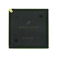
MPC561MZP56 Freescale, MPC561MZP56 Datasheet - Page 802

MPC561MZP56
Manufacturer Part Number
MPC561MZP56
Description
Manufacturer
Freescale
Datasheet
1.MPC561MZP56.pdf
(1420 pages)
Specifications of MPC561MZP56
Cpu Family
MPC56x
Device Core
PowerPC
Device Core Size
32b
Frequency (max)
56MHz
Interface Type
QSPI/SCI/SPI/UART
Total Internal Ram Size
32KB
# I/os (max)
56
Number Of Timers - General Purpose
22
Operating Supply Voltage (typ)
2.6/5V
Operating Supply Voltage (max)
2.7/5.25V
Operating Supply Voltage (min)
2.5/4.75V
On-chip Adc
2(32-chx10-bit)
Instruction Set Architecture
RISC
Operating Temp Range
-40C to 125C
Operating Temperature Classification
Automotive
Mounting
Surface Mount
Pin Count
388
Package Type
BGA
Program Memory Type
ROMLess
Program Memory Size
Not Required
Lead Free Status / RoHS Status
Not Compliant
Available stocks
Company
Part Number
Manufacturer
Quantity
Price
Company:
Part Number:
MPC561MZP56
Manufacturer:
Freescale Semiconductor
Quantity:
10 000
Company:
Part Number:
MPC561MZP56R2
Manufacturer:
Freescale Semiconductor
Quantity:
10 000
- Current page: 802 of 1420
- Download datasheet (11Mb)
Modular Input/Output Subsystem (MIOS14)
17.12.6.2 MIOS14 Interrupt Level Register 1 (MIOS14LVL1)
This register contains the interrupt level that applies to the submodules number 15 to zero.
17.13 MIOS14 Function Examples
The versatility of the MIOS14 timer architecture is based on multiple counters and capture/compare
channel units interconnected on 16-bit counter buses. This section includes some typical application
examples to show how the submodules can be interconnected to form timing functions. The diagrams used
to illustrate these examples show only the blocks utilized for that function.
To illustrate the timing range of the MIOS14 in different applications, many of the following paragraphs
include time intervals quoted in microseconds and seconds. The assumptions used are that f
MHz with minimum overall prescaling (50 ns cycle) and with the maximum overall prescaling (32 µs
cycle). For other f
scale appropriately.
17.13.1 MIOS14 Input Double Edge Pulse Width Measurement
To measure the width of an input pulse, the MIOS14 double action submodule (MDASM) has two capture
registers so that only one interrupt is needed after the second edge. The software can read both edge
17-70
SRESET
10:15
10:15
Bits
Bits
0:4
5:7
8:9
0:4
5:7
8:9
Field
Addr
MSB
Name
Name
0
LVL
LVL
TM
TM
—
—
—
—
SYS
1
Figure 17-42. MIOS14 Interrupt Level Register 1 (MIOS14LVL1)
clock cycle rates and prescaler choices, the times mentioned in these paragraphs
Reserved
Interrupt request level. This field represents one of eight possible levels.
Time multiplexing. This field determines the multiplexed time slot
Reserved
Reserved
Interrupt request level. This field represents one of eight possible levels.
Time multiplexing. This field determines the multiplexed time slot.
Reserved
—
2
3
Table 17-42. MIOS14LVL0 Bit Descriptions
Table 17-43. MIOS14LVL1 Bit Descriptions
MPC561/MPC563 Reference Manual, Rev. 1.2
4
5
LVL
0000_0000_0000_0000
6
0x30 6C70
7
Description
Description
8
TM
9
10
11
12
—
Freescale Semiconductor
13
SYS
14
is at 40
LSB
15
Related parts for MPC561MZP56
Image
Part Number
Description
Manufacturer
Datasheet
Request
R

Part Number:
Description:
MPC5 1K0 5%
Manufacturer:
TE Connectivity
Datasheet:

Part Number:
Description:
MPC5 500R 5%
Manufacturer:
TE Connectivity
Datasheet:

Part Number:
Description:
MPC5 5K0 5%
Manufacturer:
Tyco Electronics
Datasheet:

Part Number:
Description:
MPC5 5R0 5%
Manufacturer:
Tyco Electronics
Datasheet:

Part Number:
Description:
MPC5 50K 5%
Manufacturer:
Tyco Electronics
Datasheet:

Part Number:
Description:
MPC5 1R0 5%
Manufacturer:
Tyco Electronics
Datasheet:

Part Number:
Description:
TOWER ELEVATOR BOARDS HARDWARE
Manufacturer:
Freescale Semiconductor
Datasheet:

Part Number:
Description:
TOWER SERIAL I/O HARDWARE
Manufacturer:
Freescale Semiconductor
Datasheet:

Part Number:
Description:
LCD MODULE FOR TWR SYSTEM
Manufacturer:
Freescale Semiconductor
Datasheet:

Part Number:
Description:
DAUGHTER LCD WVGA I.MX51
Manufacturer:
Freescale Semiconductor
Datasheet:

Part Number:
Description:
TOWER SYSTEM BOARD MPC5125
Manufacturer:
Freescale Semiconductor
Datasheet:


