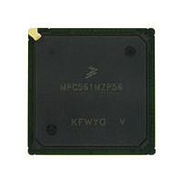
MPC561MZP56 Freescale, MPC561MZP56 Datasheet - Page 334

MPC561MZP56
Manufacturer Part Number
MPC561MZP56
Description
Manufacturer
Freescale
Datasheet
1.MPC561MZP56.pdf
(1420 pages)
Specifications of MPC561MZP56
Cpu Family
MPC56x
Device Core
PowerPC
Device Core Size
32b
Frequency (max)
56MHz
Interface Type
QSPI/SCI/SPI/UART
Total Internal Ram Size
32KB
# I/os (max)
56
Number Of Timers - General Purpose
22
Operating Supply Voltage (typ)
2.6/5V
Operating Supply Voltage (max)
2.7/5.25V
Operating Supply Voltage (min)
2.5/4.75V
On-chip Adc
2(32-chx10-bit)
Instruction Set Architecture
RISC
Operating Temp Range
-40C to 125C
Operating Temperature Classification
Automotive
Mounting
Surface Mount
Pin Count
388
Package Type
BGA
Program Memory Type
ROMLess
Program Memory Size
Not Required
Lead Free Status / RoHS Status
Not Compliant
Available stocks
Company
Part Number
Manufacturer
Quantity
Price
Company:
Part Number:
MPC561MZP56
Manufacturer:
Freescale Semiconductor
Quantity:
10 000
Company:
Part Number:
MPC561MZP56R2
Manufacturer:
Freescale Semiconductor
Quantity:
10 000
- Current page: 334 of 1420
- Download datasheet (11Mb)
Clocks and Power Control
8-32
13:14
16:17
18:23
Bits
11
12
15
ENGDIV[0:5] Engineering clock division factor. These bits define the frequency division factor between
EECLK[0:1]
EBDF[0:1]
RTSEL
Name
BUCS
LME
RTC circuit input source select. At power-on reset RTSEL receives the value of the
MODCK1 signal. Refer to
= 0), the RTSEL bit is ignored, and the backup clock is the clock source for the RT and PIT
clocks
0 OSCM clock is selected as input to RTC and PIT
1 EXTCLK clock is selected as the RTC and PIT clock source
Backup clock status. This status bit indicates the current system clock source. When loss
of clock is detected and the LME bit is set, the clock source is the backup clock and this bit
is set. When the STBUC bit and LME bit are set, the system switches to the backup clock
and BUCS is set.
0 System clock is not the backup clock
1 System clock is the backup clock
External bus division factor. These bits define the frequency division factor between
(GCLK1 and GCLK2) and (GCLK1_50 and GCLK2_50). CLKOUT is similar to GCLK2_50.
The GCLK2_50 and GCKL1_50 are used by the external bus interface and controller in
order to interface to the external system. The EBDF bits are initialized during hard reset
using the hard reset configuration mechanism.
00 CLKOUT is GCKL2 divided by 1
01 CLKOUT is GCKL2 divided by 2
1x Reserved
Note: If EBDF > 0, an external burst access with short setup timing will corrupt any USIU
Limp mode enable. When LME is set, the loss-of-clock monitor is enabled and any
detection of loss of clock will switch the system clock automatically to backup clock. It is
also possible to switch to the backup clock by setting the STBUC bit.
If LME is cleared, the option of using limp mode is disabled. The loss of clock detector is
not active, and any write to STBUC is ignored.
The LME bit is writable once, by software, after power-on reset, when the system clock is
not backup clock (BUCS = 0).
During power-on reset, the value of LME is determined by the MODCK[1:3] bits. (Refer to
Table
0 Limp mode disabled
1 Limp mode enabled
Enable engineering clock. This field controls the output buffer voltage of the ENGCLK pin.
When both bits are set the ENGCLK pin is held in the high state. These bits can be
dynamically changed without generating spikes on the ENGCLK pin. If ENGCLK is not
connected to external circuits, set both bits (disabling ENGCLK) to minimize noise and
power dissipation. For measurement purposes the backup clock (BUCLK) can be driven
externally on the ENGCLK pin.
00 Engineering clock enabled, 2.6 V output buffer
01 Engineering clock enabled (slew rate controlled), 5 V output buffer
10 BUCLK is the output on the ENGCLK 2.6 V output buffer
11 Engineering clock disabled
VCO/2 and ENGCLK. Division factor can be from 1 (ENGDIV = 000000) to 64 (ENGDIV =
111111). These bits can be read and written at any time. They are not affected by hard
reset but are cleared during power-on reset.
NOTE: If the engineering clock division factor is not a power of two, synchronization
between the system and ENGCLK is not guaranteed.
register load/store. Refer to
Table 8-9. SCCR Bit Descriptions (continued)
8-1.)
MPC561/MPC563 Reference Manual, Rev. 1.2
Table
Section 10.2.6, “Reduced Data Setup
8-1. Note that if the chip is operating in limp mode (BUCS
Description
Freescale Semiconductor
Time.”
Related parts for MPC561MZP56
Image
Part Number
Description
Manufacturer
Datasheet
Request
R

Part Number:
Description:
MPC5 1K0 5%
Manufacturer:
TE Connectivity
Datasheet:

Part Number:
Description:
MPC5 500R 5%
Manufacturer:
TE Connectivity
Datasheet:

Part Number:
Description:
MPC5 5K0 5%
Manufacturer:
Tyco Electronics
Datasheet:

Part Number:
Description:
MPC5 5R0 5%
Manufacturer:
Tyco Electronics
Datasheet:

Part Number:
Description:
MPC5 50K 5%
Manufacturer:
Tyco Electronics
Datasheet:

Part Number:
Description:
MPC5 1R0 5%
Manufacturer:
Tyco Electronics
Datasheet:

Part Number:
Description:
TOWER ELEVATOR BOARDS HARDWARE
Manufacturer:
Freescale Semiconductor
Datasheet:

Part Number:
Description:
TOWER SERIAL I/O HARDWARE
Manufacturer:
Freescale Semiconductor
Datasheet:

Part Number:
Description:
LCD MODULE FOR TWR SYSTEM
Manufacturer:
Freescale Semiconductor
Datasheet:

Part Number:
Description:
DAUGHTER LCD WVGA I.MX51
Manufacturer:
Freescale Semiconductor
Datasheet:

Part Number:
Description:
TOWER SYSTEM BOARD MPC5125
Manufacturer:
Freescale Semiconductor
Datasheet:


