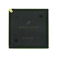
MPC561MZP56 Freescale, MPC561MZP56 Datasheet - Page 227

MPC561MZP56
Manufacturer Part Number
MPC561MZP56
Description
Manufacturer
Freescale
Datasheet
1.MPC561MZP56.pdf
(1420 pages)
Specifications of MPC561MZP56
Cpu Family
MPC56x
Device Core
PowerPC
Device Core Size
32b
Frequency (max)
56MHz
Interface Type
QSPI/SCI/SPI/UART
Total Internal Ram Size
32KB
# I/os (max)
56
Number Of Timers - General Purpose
22
Operating Supply Voltage (typ)
2.6/5V
Operating Supply Voltage (max)
2.7/5.25V
Operating Supply Voltage (min)
2.5/4.75V
On-chip Adc
2(32-chx10-bit)
Instruction Set Architecture
RISC
Operating Temp Range
-40C to 125C
Operating Temperature Classification
Automotive
Mounting
Surface Mount
Pin Count
388
Package Type
BGA
Program Memory Type
ROMLess
Program Memory Size
Not Required
Lead Free Status / RoHS Status
Not Compliant
Available stocks
Company
Part Number
Manufacturer
Quantity
Price
Company:
Part Number:
MPC561MZP56
Manufacturer:
Freescale Semiconductor
Quantity:
10 000
Company:
Part Number:
MPC561MZP56R2
Manufacturer:
Freescale Semiconductor
Quantity:
10 000
- Current page: 227 of 1420
- Download datasheet (11Mb)
4.6.2.2
The following registers contain 32 bits and define the starting address of the protected regions. There is
one register for each of four regions.
Freescale Semiconductor
,
HRESET
HRESET
1
2
27:29
20:31
BE and BTEE should not both be set at the same time, setting the BE bit disables the BTB.
This bit is available on the MPC562/MPC564 only, software should write "0" to this bit for MPC561/MPC563.
Bits
Bits
0:19
30
31
Field
Field
Addr
MSB
16
0
Region Base Address Registers (MI_RBA[0:3])
Name
When writing to the BBCMCR register, the following instruction after
mtspr BBCMCR, Rx should be ISYNC, to make sure that the programmed
value will come into effect before any further action.
RA
—
Name
DCAE
Undefined
17
TST
1
—
SPR 784 (MI_RBA0), SPR 785 (MI_RBA1), SPR 786 (MI_RBA2), SPR 787 (MI_RBA3)
RA
Region Base address. The RA field provides the base address of the region. The region base
address should start on the memory block boundary for the corresponding region size, specified
in the region attribute register MI_RA.
Reserved
18
2
Figure 4-8. Region Base Address Register (MI_RBA[0:3])
Table 4-4. BBCMCR Field Descriptions (continued)
Table 4-5. MI_RBA[0:3] Registers Bit Descriptions
Reserved.
NOTE: Bit 27 was BCMEE and should be written as 0.
Decompressor Configuration Access Enable. This bit enables DECRAM and DCCR
registers access from the U-bus master (i.e., RCPU, external master).
0 DECRAM and DCCR registers are locked.
1 DECRAM allows accesses from the U-bus only.
DCAE bit should be set before vocabulary tables are loaded via the U-bus.
Reserved for BBC Test Operations.
19
3
MPC561/MPC563 Reference Manual, Rev. 1.2
20
4
21
5
22
6
NOTE
Unchanged
23
7
RA
Description
24
8
Description
0000_0000_0000
25
9
—
10
26
11
27
Burst Buffer Controller 2 Module
12
28
13
29
14
30
LSB
15
31
4-21
Related parts for MPC561MZP56
Image
Part Number
Description
Manufacturer
Datasheet
Request
R

Part Number:
Description:
MPC5 1K0 5%
Manufacturer:
TE Connectivity
Datasheet:

Part Number:
Description:
MPC5 500R 5%
Manufacturer:
TE Connectivity
Datasheet:

Part Number:
Description:
MPC5 5K0 5%
Manufacturer:
Tyco Electronics
Datasheet:

Part Number:
Description:
MPC5 5R0 5%
Manufacturer:
Tyco Electronics
Datasheet:

Part Number:
Description:
MPC5 50K 5%
Manufacturer:
Tyco Electronics
Datasheet:

Part Number:
Description:
MPC5 1R0 5%
Manufacturer:
Tyco Electronics
Datasheet:

Part Number:
Description:
TOWER ELEVATOR BOARDS HARDWARE
Manufacturer:
Freescale Semiconductor
Datasheet:

Part Number:
Description:
TOWER SERIAL I/O HARDWARE
Manufacturer:
Freescale Semiconductor
Datasheet:

Part Number:
Description:
LCD MODULE FOR TWR SYSTEM
Manufacturer:
Freescale Semiconductor
Datasheet:

Part Number:
Description:
DAUGHTER LCD WVGA I.MX51
Manufacturer:
Freescale Semiconductor
Datasheet:

Part Number:
Description:
TOWER SYSTEM BOARD MPC5125
Manufacturer:
Freescale Semiconductor
Datasheet:


