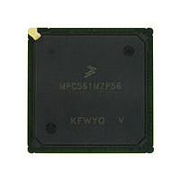
MPC561MZP56 Freescale, MPC561MZP56 Datasheet - Page 531

MPC561MZP56
Manufacturer Part Number
MPC561MZP56
Description
Manufacturer
Freescale
Datasheet
1.MPC561MZP56.pdf
(1420 pages)
Specifications of MPC561MZP56
Cpu Family
MPC56x
Device Core
PowerPC
Device Core Size
32b
Frequency (max)
56MHz
Interface Type
QSPI/SCI/SPI/UART
Total Internal Ram Size
32KB
# I/os (max)
56
Number Of Timers - General Purpose
22
Operating Supply Voltage (typ)
2.6/5V
Operating Supply Voltage (max)
2.7/5.25V
Operating Supply Voltage (min)
2.5/4.75V
On-chip Adc
2(32-chx10-bit)
Instruction Set Architecture
RISC
Operating Temp Range
-40C to 125C
Operating Temperature Classification
Automotive
Mounting
Surface Mount
Pin Count
388
Package Type
BGA
Program Memory Type
ROMLess
Program Memory Size
Not Required
Lead Free Status / RoHS Status
Not Compliant
Available stocks
Company
Part Number
Manufacturer
Quantity
Price
Company:
Part Number:
MPC561MZP56
Manufacturer:
Freescale Semiconductor
Quantity:
10 000
Company:
Part Number:
MPC561MZP56R2
Manufacturer:
Freescale Semiconductor
Quantity:
10 000
- Current page: 531 of 1420
- Download datasheet (11Mb)
Port A signals are configured as inputs or outputs by programming the port data direction register,
DDRQA. The digital input signal states are read from the port data register, PORTQA, when the port data
direction register specifies that the signals are inputs. The digital data in the port data register is driven onto
the port A signals when the corresponding bit in the port data direction register specifies that the signals
are outputs. Refer to
configured as push-pull drivers, external pull-up provisions are not necessary when the output is used to
drive another integrated circuit.
13.7.2
The QADC64E uses two external trigger signals (ETRIG[2:1]). Each of the two input external trigger
signals is associated with one of the scan queues, queue 1 or queue 2 The assignment of ETRIG[2:1] to a
queue is made in the QACR0 register by the TRG bit. When TRG=0, ETRIG[1] triggers queue 1 and
ETRIG[2] triggers queue 2. When TRG=1, ETRIG[1] triggers queue 2 and ETRIG[2] triggers queue 1.
13.7.3
V
power is required to isolate the sensitive analog circuitry from the normal levels of noise present on the
digital power supply. Refer to
The analog supply signals (V
V
Freescale Semiconductor
DDA
RL
) and of the analog multiplexer inputs.
and V
External Trigger Input Signals
Analog Power Signals
SSA
The ETRIG[2:1] pins on the MPC561/MPC563 are multiplexed with the
PCS[7:6] pins.
signals supply power to the analog subsystems of the QADC64E module. Dedicated
Appendix B, “Internal Memory
DDA
Appendix F, “Electrical
MPC561/MPC563 Reference Manual, Rev. 1.2
and V
SSA
) define the limits of the analog reference voltages (V
Figure 13-49
NOTE
Map,” for more information. Since the outputs are
Characteristics,” for more information.
is a diagram of the analog input circuitry.
QADC64E Legacy Mode Operation
RH
and
13-67
Related parts for MPC561MZP56
Image
Part Number
Description
Manufacturer
Datasheet
Request
R

Part Number:
Description:
MPC5 1K0 5%
Manufacturer:
TE Connectivity
Datasheet:

Part Number:
Description:
MPC5 500R 5%
Manufacturer:
TE Connectivity
Datasheet:

Part Number:
Description:
MPC5 5K0 5%
Manufacturer:
Tyco Electronics
Datasheet:

Part Number:
Description:
MPC5 5R0 5%
Manufacturer:
Tyco Electronics
Datasheet:

Part Number:
Description:
MPC5 50K 5%
Manufacturer:
Tyco Electronics
Datasheet:

Part Number:
Description:
MPC5 1R0 5%
Manufacturer:
Tyco Electronics
Datasheet:

Part Number:
Description:
TOWER ELEVATOR BOARDS HARDWARE
Manufacturer:
Freescale Semiconductor
Datasheet:

Part Number:
Description:
TOWER SERIAL I/O HARDWARE
Manufacturer:
Freescale Semiconductor
Datasheet:

Part Number:
Description:
LCD MODULE FOR TWR SYSTEM
Manufacturer:
Freescale Semiconductor
Datasheet:

Part Number:
Description:
DAUGHTER LCD WVGA I.MX51
Manufacturer:
Freescale Semiconductor
Datasheet:

Part Number:
Description:
TOWER SYSTEM BOARD MPC5125
Manufacturer:
Freescale Semiconductor
Datasheet:


