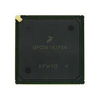
MPC561MZP56 Freescale, MPC561MZP56 Datasheet - Page 150

MPC561MZP56
Manufacturer Part Number
MPC561MZP56
Description
Manufacturer
Freescale
Datasheet
1.MPC561MZP56.pdf
(1420 pages)
Specifications of MPC561MZP56
Cpu Family
MPC56x
Device Core
PowerPC
Device Core Size
32b
Frequency (max)
56MHz
Interface Type
QSPI/SCI/SPI/UART
Total Internal Ram Size
32KB
# I/os (max)
56
Number Of Timers - General Purpose
22
Operating Supply Voltage (typ)
2.6/5V
Operating Supply Voltage (max)
2.7/5.25V
Operating Supply Voltage (min)
2.5/4.75V
On-chip Adc
2(32-chx10-bit)
Instruction Set Architecture
RISC
Operating Temp Range
-40C to 125C
Operating Temperature Classification
Automotive
Mounting
Surface Mount
Pin Count
388
Package Type
BGA
Program Memory Type
ROMLess
Program Memory Size
Not Required
Lead Free Status / RoHS Status
Not Compliant
Available stocks
Company
Part Number
Manufacturer
Quantity
Price
Company:
Part Number:
MPC561MZP56
Manufacturer:
Freescale Semiconductor
Quantity:
10 000
Company:
Part Number:
MPC561MZP56R2
Manufacturer:
Freescale Semiconductor
Quantity:
10 000
- Current page: 150 of 1420
- Download datasheet (11Mb)
Central Processing Unit
on consecutive clock cycles. Divide instructions are not pipelined; an integer divide instruction preceded
or followed by an integer divide or multiply instruction results in a processor-pipeline stall. However, since
IMUL–IDIV and ALU–BFU are implemented as separate execution units, an integer divide instruction
preceded or followed by an ALU–BFU instruction does not cause a delay in the pipeline.
3.4.3
The load/store unit handles all data transfer between the general-purpose register file and the internal
load/store bus (L-bus). The load/store unit is implemented as an independent execution unit so that stalls
in the memory pipeline do not stall the master instruction pipeline (unless there is a data dependency). The
unit is fully pipelined so that memory instructions of any size may be issued on back-to-back cycles.
There is a 32-bit wide data path between the load/store unit and the general-purpose register file.
Single-word accesses can be achieved with an internal on-chip data RAM, resulting in a two-clock latency.
Double-word accesses require two clocks, resulting in a three-clock latency. Since the L-bus is 32 bits
wide, double-word transfers require two bus accesses. The load/store unit performs zero-fill for byte and
half-word transfers and sign extension for half-word transfers.
Addresses are formed by adding the source-one register operand specified by the instruction (or zero) to
either a source-two register operand or to a 16-bit, immediate value embedded in the instruction.
3.4.4
The FPU contains a double-precision multiply array, the floating-point status and control register
(FPSCR), and the FPRs. The multiply-add array allows the RCPU to efficiently implement floating-point
operations such as multiply, multiply-add, and divide.
The RCPU depends on a software envelope to fully implement the IEEE floating-point specification.
Overflows, underflows, NaNs (not a number), and denormalized numbers cause floating-point assist
exceptions that invoke a software routine to deliver (with hardware assistance) the correct IEEE result.
To accelerate time-critical operations and make them more deterministic, the RCPU provides a mode of
operation that avoids invoking a software envelope and attempts to deliver results in hardware that are
adequate for most applications, if not in strict compliance with IEEE standards. In this mode, denormalized
numbers, NaNs, and IEEE invalid operations are legitimate, returning default results rather than causing
floating-point assist exceptions.
3.5
The PowerPC ISA architecture consists of three levels:
3-6
•
•
User instruction set architecture (UISA) — defines the base user-level instruction set, user-level
registers, data types, floating-point exception model, memory models for a uniprocessor
environment, and programming model for a uniprocessor environment.
Virtual environment architecture (VEA) — describes the memory model for a multiprocessor
environment, and describes other aspects of virtual environments.
Implementations that conform to the VEA also adhere to the UISA, but may not necessarily adhere
to the OEA.
Levels of the PowerPC ISA Architecture
Load/Store Unit (LSU)
Floating-Point Unit (FPU)
MPC561/MPC563 Reference Manual, Rev. 1.2
Freescale Semiconductor
Related parts for MPC561MZP56
Image
Part Number
Description
Manufacturer
Datasheet
Request
R

Part Number:
Description:
MPC5 1K0 5%
Manufacturer:
TE Connectivity
Datasheet:

Part Number:
Description:
MPC5 500R 5%
Manufacturer:
TE Connectivity
Datasheet:

Part Number:
Description:
MPC5 5K0 5%
Manufacturer:
Tyco Electronics
Datasheet:

Part Number:
Description:
MPC5 5R0 5%
Manufacturer:
Tyco Electronics
Datasheet:

Part Number:
Description:
MPC5 50K 5%
Manufacturer:
Tyco Electronics
Datasheet:

Part Number:
Description:
MPC5 1R0 5%
Manufacturer:
Tyco Electronics
Datasheet:

Part Number:
Description:
TOWER ELEVATOR BOARDS HARDWARE
Manufacturer:
Freescale Semiconductor
Datasheet:

Part Number:
Description:
TOWER SERIAL I/O HARDWARE
Manufacturer:
Freescale Semiconductor
Datasheet:

Part Number:
Description:
LCD MODULE FOR TWR SYSTEM
Manufacturer:
Freescale Semiconductor
Datasheet:

Part Number:
Description:
DAUGHTER LCD WVGA I.MX51
Manufacturer:
Freescale Semiconductor
Datasheet:

Part Number:
Description:
TOWER SYSTEM BOARD MPC5125
Manufacturer:
Freescale Semiconductor
Datasheet:


