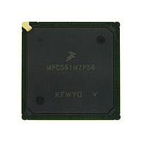
MPC561MZP56 Freescale, MPC561MZP56 Datasheet - Page 578

MPC561MZP56
Manufacturer Part Number
MPC561MZP56
Description
Manufacturer
Freescale
Datasheet
1.MPC561MZP56.pdf
(1420 pages)
Specifications of MPC561MZP56
Cpu Family
MPC56x
Device Core
PowerPC
Device Core Size
32b
Frequency (max)
56MHz
Interface Type
QSPI/SCI/SPI/UART
Total Internal Ram Size
32KB
# I/os (max)
56
Number Of Timers - General Purpose
22
Operating Supply Voltage (typ)
2.6/5V
Operating Supply Voltage (max)
2.7/5.25V
Operating Supply Voltage (min)
2.5/4.75V
On-chip Adc
2(32-chx10-bit)
Instruction Set Architecture
RISC
Operating Temp Range
-40C to 125C
Operating Temperature Classification
Automotive
Mounting
Surface Mount
Pin Count
388
Package Type
BGA
Program Memory Type
ROMLess
Program Memory Size
Not Required
Lead Free Status / RoHS Status
Not Compliant
Available stocks
Company
Part Number
Manufacturer
Quantity
Price
Company:
Part Number:
MPC561MZP56
Manufacturer:
Freescale Semiconductor
Quantity:
10 000
Company:
Part Number:
MPC561MZP56R2
Manufacturer:
Freescale Semiconductor
Quantity:
10 000
- Current page: 578 of 1420
- Download datasheet (11Mb)
QADC64E Enhanced Mode Operation
14.3.10.1 Analog Subsystem
This section describes the QADC64E analog subsystem, which includes the front-end analog multiplexer
and analog-to-digital converter.
14.3.11 Analog-to-Digital Converter Operation
The analog subsystem consists of the path from the input signals to the A/D converter block. Signals from
the queue control logic are fed to the multiplexer and state machine. The end of convert (EOC) signal and
the successive-approximation register (SAR) are the result of the conversion.
diagram of the QADC64E analog subsystem.
14.3.11.1 Conversion Cycle Times
Total conversion time is made up of initial sample time, final sample time, and resolution time. Initial
sample time refers to the time during which the selected input channel is coupled through the buffer
amplifier to the sample capacitor. This buffer is used to quickly reproduce its input signal on the sample
capacitor and minimize charge sharing errors. During the final sampling period the amplifier is bypassed,
and the multiplexer input charges the sample capacitor array directly for improved accuracy. During the
resolution period, the voltage in the sample capacitor is converted to a digital value and stored in the SAR.
Initial sample time is fixed at two QCLK cycles. Final sample time can be two or eight QCLK cycles,
depending on the value of the IST field in the CCW. Resolution time is ten QCLK cycles.
14-36
ALTREF
AN44
AN59
V
V
.
. .
RH
RL
Figure 14-20. QADC64E Analog Subsystem Block Diagram
CCW Buffer
Data Bus
CHAN
Decoder
7
10
MPC561/MPC563 Reference Manual, Rev. 1.2
Sample
REF
IST
+
-
Result
Buffer
AMP
State Mach, SAR and SAR Buffer
RDAC
(7 BIT)
7
Standard Converter Interface
CONV.
Final
Buffer
WCCW EOS/EOC
STOP
Sample
CAP Array
Equals CDAC
CRH
CRL
CDAC
(4 BIT)
4 (one is offset)
CLK
BIAS
Figure 14-20
-
+
COMP.
Zero
Freescale Semiconductor
2
shows a block
Related parts for MPC561MZP56
Image
Part Number
Description
Manufacturer
Datasheet
Request
R

Part Number:
Description:
MPC5 1K0 5%
Manufacturer:
TE Connectivity
Datasheet:

Part Number:
Description:
MPC5 500R 5%
Manufacturer:
TE Connectivity
Datasheet:

Part Number:
Description:
MPC5 5K0 5%
Manufacturer:
Tyco Electronics
Datasheet:

Part Number:
Description:
MPC5 5R0 5%
Manufacturer:
Tyco Electronics
Datasheet:

Part Number:
Description:
MPC5 50K 5%
Manufacturer:
Tyco Electronics
Datasheet:

Part Number:
Description:
MPC5 1R0 5%
Manufacturer:
Tyco Electronics
Datasheet:

Part Number:
Description:
TOWER ELEVATOR BOARDS HARDWARE
Manufacturer:
Freescale Semiconductor
Datasheet:

Part Number:
Description:
TOWER SERIAL I/O HARDWARE
Manufacturer:
Freescale Semiconductor
Datasheet:

Part Number:
Description:
LCD MODULE FOR TWR SYSTEM
Manufacturer:
Freescale Semiconductor
Datasheet:

Part Number:
Description:
DAUGHTER LCD WVGA I.MX51
Manufacturer:
Freescale Semiconductor
Datasheet:

Part Number:
Description:
TOWER SYSTEM BOARD MPC5125
Manufacturer:
Freescale Semiconductor
Datasheet:


