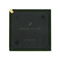
MPC561MZP56 Freescale, MPC561MZP56 Datasheet - Page 672

MPC561MZP56
Manufacturer Part Number
MPC561MZP56
Description
Manufacturer
Freescale
Datasheet
1.MPC561MZP56.pdf
(1420 pages)
Specifications of MPC561MZP56
Cpu Family
MPC56x
Device Core
PowerPC
Device Core Size
32b
Frequency (max)
56MHz
Interface Type
QSPI/SCI/SPI/UART
Total Internal Ram Size
32KB
# I/os (max)
56
Number Of Timers - General Purpose
22
Operating Supply Voltage (typ)
2.6/5V
Operating Supply Voltage (max)
2.7/5.25V
Operating Supply Voltage (min)
2.5/4.75V
On-chip Adc
2(32-chx10-bit)
Instruction Set Architecture
RISC
Operating Temp Range
-40C to 125C
Operating Temperature Classification
Automotive
Mounting
Surface Mount
Pin Count
388
Package Type
BGA
Program Memory Type
ROMLess
Program Memory Size
Not Required
Lead Free Status / RoHS Status
Not Compliant
Available stocks
Company
Part Number
Manufacturer
Quantity
Price
Company:
Part Number:
MPC561MZP56
Manufacturer:
Freescale Semiconductor
Quantity:
10 000
Company:
Part Number:
MPC561MZP56R2
Manufacturer:
Freescale Semiconductor
Quantity:
10 000
- Current page: 672 of 1420
- Download datasheet (11Mb)
Queued Serial Multi-Channel Module
15.7.7.5
The transmitter consists of a serial shifter and a parallel data register (TDRx) located in the SCI data
register (SCxDR). The serial shifter cannot be directly accessed by the CPU. The transmitter is
double-buffered, which means that data can be loaded into the TDRx while other data is shifted out. The
TE bit in SCCxR1 enables (TE = 1) and disables (TE = 0) the transmitter.
The shifter output is connected to the TXD pin while the transmitter is operating (TE = 1, or TE = 0 and
transmission in progress). Wired-OR operation should be specified when more than one transmitter is used
on the same SCI bus. The WOMS bit in SCCxR1 determines whether TXD is an open drain (wired-OR)
output or a normal CMOS output. An external pull-up resistor on TXD is necessary for wired-OR
operation. WOMS controls TXD function, regardless of whether the pin is used by the SCI or as a
general-purpose output pin.
Data to be transmitted is written to SCxDR, then transferred to the serial shifter. Before writing to TDRx,
the transmit data register empty (TDRE) flag in SCxSR should be checked. When TDRE = 0, the TDRx
contains data that has not been transferred to the shifter. Writing to SCxDR again overwrites the data. If
TDRE = 1, then TDRx is empty, and new data may be written to TDRx, clearing TDRE.
As soon as the data in the transmit serial shifter has shifted out and if a new data frame is in TDRx (TDRE
= 0), then the new data is transferred from TDRx to the transmit serial shifter and TDRE is set
automatically. An interrupt may optionally be generated at this point.
The transmission complete (TC) flag in SCxSR shows transmitter shifter state. When TC = 0, the shifter
is busy. TC is set when all shifting operations are completed. TC is not automatically cleared. The
processor must clear it by first reading SCxSR while TC is set, then writing new data to SCxDR, or writing
to SCTQ[0:15] for transmit queue operation.
The state of the serial shifter is checked when the TE bit is set. If TC = 1, an idle frame is transmitted as a
preamble to the following data frame. If TC = 0, the current operation continues until the final bit in the
frame is sent, then the preamble is transmitted. The TC bit is set at the end of preamble transmission.
The SBK bit in SCCxR1 is used to insert break frames in a transmission. A non-zero integer number of
break frames are transmitted while SBK is set. Break transmission begins when SBK is set, and ends with
the transmission in progress at the time either SBK or TE is cleared. If SBK is set while a transmission is
in progress, that transmission finishes normally before the break begins. To ensure the minimum break
time, toggle SBK quickly to one and back to zero. The TC bit is set at the end of break transmission. After
break transmission, at least one bit-time of logic level one (mark idle) is transmitted to ensure that a
subsequent start bit can be detected.
If TE remains set, after all pending idle, data and break frames are shifted out, TDRE and TC are set and
TXD is held at logic level one (mark).
15-54
Transmitter Operation
Table 15-31. Effect of Parity Checking on Data Size
M
1
1
MPC561/MPC563 Reference Manual, Rev. 1.2
PE
0
1
9 data bits
8 data bits, 1 parity bit
Result
Freescale Semiconductor
Related parts for MPC561MZP56
Image
Part Number
Description
Manufacturer
Datasheet
Request
R

Part Number:
Description:
MPC5 1K0 5%
Manufacturer:
TE Connectivity
Datasheet:

Part Number:
Description:
MPC5 500R 5%
Manufacturer:
TE Connectivity
Datasheet:

Part Number:
Description:
MPC5 5K0 5%
Manufacturer:
Tyco Electronics
Datasheet:

Part Number:
Description:
MPC5 5R0 5%
Manufacturer:
Tyco Electronics
Datasheet:

Part Number:
Description:
MPC5 50K 5%
Manufacturer:
Tyco Electronics
Datasheet:

Part Number:
Description:
MPC5 1R0 5%
Manufacturer:
Tyco Electronics
Datasheet:

Part Number:
Description:
TOWER ELEVATOR BOARDS HARDWARE
Manufacturer:
Freescale Semiconductor
Datasheet:

Part Number:
Description:
TOWER SERIAL I/O HARDWARE
Manufacturer:
Freescale Semiconductor
Datasheet:

Part Number:
Description:
LCD MODULE FOR TWR SYSTEM
Manufacturer:
Freescale Semiconductor
Datasheet:

Part Number:
Description:
DAUGHTER LCD WVGA I.MX51
Manufacturer:
Freescale Semiconductor
Datasheet:

Part Number:
Description:
TOWER SYSTEM BOARD MPC5125
Manufacturer:
Freescale Semiconductor
Datasheet:


