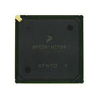
MPC561MZP56 Freescale, MPC561MZP56 Datasheet - Page 1226

MPC561MZP56
Manufacturer Part Number
MPC561MZP56
Description
Manufacturer
Freescale
Datasheet
1.MPC561MZP56.pdf
(1420 pages)
Specifications of MPC561MZP56
Cpu Family
MPC56x
Device Core
PowerPC
Device Core Size
32b
Frequency (max)
56MHz
Interface Type
QSPI/SCI/SPI/UART
Total Internal Ram Size
32KB
# I/os (max)
56
Number Of Timers - General Purpose
22
Operating Supply Voltage (typ)
2.6/5V
Operating Supply Voltage (max)
2.7/5.25V
Operating Supply Voltage (min)
2.5/4.75V
On-chip Adc
2(32-chx10-bit)
Instruction Set Architecture
RISC
Operating Temp Range
-40C to 125C
Operating Temperature Classification
Automotive
Mounting
Surface Mount
Pin Count
388
Package Type
BGA
Program Memory Type
ROMLess
Program Memory Size
Not Required
Lead Free Status / RoHS Status
Not Compliant
Available stocks
Company
Part Number
Manufacturer
Quantity
Price
Company:
Part Number:
MPC561MZP56
Manufacturer:
Freescale Semiconductor
Quantity:
10 000
Company:
Part Number:
MPC561MZP56R2
Manufacturer:
Freescale Semiconductor
Quantity:
10 000
- Current page: 1226 of 1420
- Download datasheet (11Mb)
Electrical Characteristics
F-10
1
2
3
4
5
6
7
8
9
10
11
12
13
14
15
16
17
53a IRAMSTBY Regulator Current Data Retention
53b IRAMSTBY Regulator Voltage for Data Retention
53
54
55
56
57
This characteristic is for 2.6-V output and 5-V input friendly pins.
VDATAPC is the maximum voltage the data pins can have been precharged to by an external device when the
MPC561/MPC563 data pins turn on as outputs. The 3.1-V maximum for VDATAPC is to allow the data pins to be driven
from an external memory running at a higher voltage. Note that if the data pins are precharged to higher than V
then the 50-pF maximum load characteristic must be observed.
The predischarge circuit is enabled by setting the PREDIS_EN bit to a “1” in the PDMCR2 register. VDATAPC is the
maximum voltage the data pins can have been precharged to by an external device when the MPC561/MPC563 data
pins turn on as outputs. The 5.25-V maximum for VDATAPC is to allow the data pins to be driven from an external
memory running at a higher voltage. Note that if the data pins are precharged to higher than V
load characteristic must match the data bus drive setting and the data bus can withstand up to 3.6 volts for a cumulative
time of 24 hours over the lifetime of the device.
This characteristic is for 5-V output and 5-V input pins.
0.3V > V
Within this range, no significant injection will be seen. See QADC64 Disruptive Input Current (I
During reset all 2.6V and 2.6V/5V pads will leak up to 10µA to QVDDL if the pad has a voltage > QVDDL.
Maximum leakage occurs at maximum operating temperature. Current decreases by approximately one-half for each
8 to 12 °C, in the ambient temperature range of 50 to 125 °C.
All bus pins support two drive strengths capabilities, 25 pF and 50 pF. Current drive is less at the 25-pF
capacitive load. Both modes achieve 40-MHz (or, optionally, 56-MHz) timing.
Only IRQ, TPU, MIOS, GPIO, QADC (when digital inputs) and RESET pins have hysteresis, thus there is no hysteresis
specification on all other pins
Values to be characterized. Current consumption values will be updated as information becomes available. Initial
values are only estimates based on predicted capacitive differences between CDR1 and CDR3 as well as actual CDR1
measurements.
All power consumption specifications assume 50-pF loads and running a typical application. The power consumption
of some modules could go up if they are exercised heavier, but the power consumption of other modules would
decrease.
This value depends on the R value set by the user. Refer to
These power supplies are available on the MPC563 and MPC564 only.
Current measured at maximum system clock frequency with QADC active.
Transient currents can reach 50mA.
KAPWR and IRAMSTBY can be powered-up prior to any other supply or at the same time as the other 2.6 V supplies.
IRAMSTBY must lead or coincide with VDD; however it can lag KAPWR.
Standby Supply Current
KAPWR only (4 MHz Crystal)
KAPWR only (20 MHz Crystal)
Measured @ 2.7 V
Specified V
(power-down mode) Specified V
(V
DC Injection Current per Pin GPIO, TPU, MIOS, QSMCM,
EPEE and 5 V pins
DC Injection Current per Pin 2.6 V
QADC64 Disruptive Input Current
Power Dissipation – 56 MHz
40 MHz
DD
DDA
, V
DDH
or V
DD
= V
DDH
applied (V
SS
, whichever is greater.
)
21
6, 23, 24
Characteristic
Table F-4. DC Electrical Characteristics (continued)
DD
, V
MPC561/MPC563 Reference Manual, Rev. 1.2
DDH
DD
24,27
= V
6, 24, 25, 26
applied
SS
)
17
17,22
Appendix C, “Clock and Board
ISB
ISB
Symbol
V
I
KAPWR20
I
STBY
KAPWR4
STBY
I
IC26
I
PD
IC5
NA
50 x 10
1.35
Min
-1.0
-1.0
- 3
—
Guidelines.”
-3
DDL
NA
Freescale Semiconductor
, then the maximum
).
Max
1.75
1.95
1.12
2.0
1.0
1.0
0.8
5
3
DDL
Unit
mΑ
mΑ
mA
mA
mA
mA
W
W
V
,
Related parts for MPC561MZP56
Image
Part Number
Description
Manufacturer
Datasheet
Request
R

Part Number:
Description:
MPC5 1K0 5%
Manufacturer:
TE Connectivity
Datasheet:

Part Number:
Description:
MPC5 500R 5%
Manufacturer:
TE Connectivity
Datasheet:

Part Number:
Description:
MPC5 5K0 5%
Manufacturer:
Tyco Electronics
Datasheet:

Part Number:
Description:
MPC5 5R0 5%
Manufacturer:
Tyco Electronics
Datasheet:

Part Number:
Description:
MPC5 50K 5%
Manufacturer:
Tyco Electronics
Datasheet:

Part Number:
Description:
MPC5 1R0 5%
Manufacturer:
Tyco Electronics
Datasheet:

Part Number:
Description:
TOWER ELEVATOR BOARDS HARDWARE
Manufacturer:
Freescale Semiconductor
Datasheet:

Part Number:
Description:
TOWER SERIAL I/O HARDWARE
Manufacturer:
Freescale Semiconductor
Datasheet:

Part Number:
Description:
LCD MODULE FOR TWR SYSTEM
Manufacturer:
Freescale Semiconductor
Datasheet:

Part Number:
Description:
DAUGHTER LCD WVGA I.MX51
Manufacturer:
Freescale Semiconductor
Datasheet:

Part Number:
Description:
TOWER SYSTEM BOARD MPC5125
Manufacturer:
Freescale Semiconductor
Datasheet:


