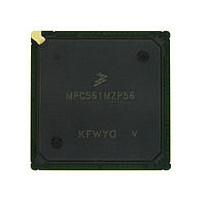
MPC561MZP56 Freescale, MPC561MZP56 Datasheet - Page 499

MPC561MZP56
Manufacturer Part Number
MPC561MZP56
Description
Manufacturer
Freescale
Datasheet
1.MPC561MZP56.pdf
(1420 pages)
Specifications of MPC561MZP56
Cpu Family
MPC56x
Device Core
PowerPC
Device Core Size
32b
Frequency (max)
56MHz
Interface Type
QSPI/SCI/SPI/UART
Total Internal Ram Size
32KB
# I/os (max)
56
Number Of Timers - General Purpose
22
Operating Supply Voltage (typ)
2.6/5V
Operating Supply Voltage (max)
2.7/5.25V
Operating Supply Voltage (min)
2.5/4.75V
On-chip Adc
2(32-chx10-bit)
Instruction Set Architecture
RISC
Operating Temp Range
-40C to 125C
Operating Temperature Classification
Automotive
Mounting
Surface Mount
Pin Count
388
Package Type
BGA
Program Memory Type
ROMLess
Program Memory Size
Not Required
Lead Free Status / RoHS Status
Not Compliant
Available stocks
Company
Part Number
Manufacturer
Quantity
Price
Company:
Part Number:
MPC561MZP56
Manufacturer:
Freescale Semiconductor
Quantity:
10 000
Company:
Part Number:
MPC561MZP56R2
Manufacturer:
Freescale Semiconductor
Quantity:
10 000
- Current page: 499 of 1420
- Download datasheet (11Mb)
13.4.1.1
Total conversion time is made up of initial sample time, final sample time, and resolution time. Initial
sample time refers to the time during which the selected input channel is coupled through the buffer
amplifier to the sample capacitor. This buffer is used to quickly reproduce its input signal on the sample
capacitor and minimize charge sharing errors. During the final sampling period the amplifier is bypassed,
and the multiplexer input charges the sample capacitor array directly for improved accuracy. During the
resolution period, the voltage in the sample capacitor is converted to a digital value and stored in the SAR.
Initial sample time is fixed at two QCLK cycles. Final sample time can be 2, 4, 6, 8, or 16 QCLK cycles,
depending on the value of the IST field in the CCW. Resolution time is ten QCLK cycles.
Therefore, conversion time requires a minimum of 14 QCLK clocks (7 µs with a 2.0-MHz QCLK). If the
maximum final sample time period of 16 QCLKs is selected, the total conversion time is 28 QCLKs or 14
µs (with a 2.0-MHz QCLK)
Figure 13-21
13.4.1.2
If the amplifier bypass mode is enabled for a conversion by setting the amplifier bypass (BYP) bit in the
CCW, the timing changes to that shown in
the potential conversion time by two QCLKs. However, due to internal RC effects, a minimum final
sample time of four QCLKs must be allowed. This results in no savings of QCLKs. When using the bypass
mode, the external circuit should be of low source impedance, typically less than 10 kΩ. Also, the loading
effects of the external circuitry by the QADC64E need to be considered, since the benefits of the sample
amplifier are not present.
Freescale Semiconductor
QCLK
Conversion Cycle Times
Amplifier Bypass Mode Conversion Timing
illustrates the timing for conversions.
Because of internal RC time constants, a sample time of two QCLKs in
bypass mode for high frequency operation is not recommended.
2 cycles
Sample
BUFFER
Time
Sample TIME
Final Sample
(2, 4, 8, 16)
N cycles:
MPC561/MPC563 Reference Manual, Rev. 1.2
Time
Figure 13-21. Conversion Timing
Figure
Successive Approximation Resolution
13-22. The buffered sample time is eliminated, reducing
NOTE
Sequence
Resolution
10 cycles
Time
QADC64E Legacy Mode Operation
13-35
Related parts for MPC561MZP56
Image
Part Number
Description
Manufacturer
Datasheet
Request
R

Part Number:
Description:
MPC5 1K0 5%
Manufacturer:
TE Connectivity
Datasheet:

Part Number:
Description:
MPC5 500R 5%
Manufacturer:
TE Connectivity
Datasheet:

Part Number:
Description:
MPC5 5K0 5%
Manufacturer:
Tyco Electronics
Datasheet:

Part Number:
Description:
MPC5 5R0 5%
Manufacturer:
Tyco Electronics
Datasheet:

Part Number:
Description:
MPC5 50K 5%
Manufacturer:
Tyco Electronics
Datasheet:

Part Number:
Description:
MPC5 1R0 5%
Manufacturer:
Tyco Electronics
Datasheet:

Part Number:
Description:
TOWER ELEVATOR BOARDS HARDWARE
Manufacturer:
Freescale Semiconductor
Datasheet:

Part Number:
Description:
TOWER SERIAL I/O HARDWARE
Manufacturer:
Freescale Semiconductor
Datasheet:

Part Number:
Description:
LCD MODULE FOR TWR SYSTEM
Manufacturer:
Freescale Semiconductor
Datasheet:

Part Number:
Description:
DAUGHTER LCD WVGA I.MX51
Manufacturer:
Freescale Semiconductor
Datasheet:

Part Number:
Description:
TOWER SYSTEM BOARD MPC5125
Manufacturer:
Freescale Semiconductor
Datasheet:


