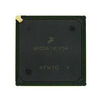
MPC561MZP56 Freescale, MPC561MZP56 Datasheet - Page 332

MPC561MZP56
Manufacturer Part Number
MPC561MZP56
Description
Manufacturer
Freescale
Datasheet
1.MPC561MZP56.pdf
(1420 pages)
Specifications of MPC561MZP56
Cpu Family
MPC56x
Device Core
PowerPC
Device Core Size
32b
Frequency (max)
56MHz
Interface Type
QSPI/SCI/SPI/UART
Total Internal Ram Size
32KB
# I/os (max)
56
Number Of Timers - General Purpose
22
Operating Supply Voltage (typ)
2.6/5V
Operating Supply Voltage (max)
2.7/5.25V
Operating Supply Voltage (min)
2.5/4.75V
On-chip Adc
2(32-chx10-bit)
Instruction Set Architecture
RISC
Operating Temp Range
-40C to 125C
Operating Temperature Classification
Automotive
Mounting
Surface Mount
Pin Count
388
Package Type
BGA
Program Memory Type
ROMLess
Program Memory Size
Not Required
Lead Free Status / RoHS Status
Not Compliant
Available stocks
Company
Part Number
Manufacturer
Quantity
Price
Company:
Part Number:
MPC561MZP56
Manufacturer:
Freescale Semiconductor
Quantity:
10 000
Company:
Part Number:
MPC561MZP56R2
Manufacturer:
Freescale Semiconductor
Quantity:
10 000
- Current page: 332 of 1420
- Download datasheet (11Mb)
1
2
3
4
PORESET
PORESET
The hard reset value is a reset configuration word value, extracted from the indicated internal data bus lines. Refer to
EQ2 = MODCK1
EQ3 = (MODCK1 AND MODCK2 AND MODCK3) | (MODCK1 AND MODCK2 AND MODCK3) | (MODCK1 AND MODCK2 AND
RTDIV will be 0 if MODCK[1:3] = 000.
HRESET
HRESET
“Hard Reset Configuration Word
MODCK3). See
Clocks and Power Control
8-30
Field DBCT
Addr
Bits
1:2
EECLK[0:1]
0
MSB
16
U
0
1
0
Table
17
0
0
0
1
COM[1] bit default value is determined during by BDRV reset
configuration bit; See
(RCW).”
COM
Name
DBCT
COM
8-1.
ID2
ID2
18
1
2
Figure 8-16. System Clock and Reset Control Register (SCCR)
1
1
DCSLR MFPDL LPML TBS RTDIV
(RCW).”
Disable backup clock for timers. The DBCT bit controls the timers clock source while the
chip is in limp mode. If DBCT is set, the timers clock (TMBLCK, PITRCLK) source will not
be the backup clock, even if the system clock source is the backup clock ring oscillator. The
real-time clock source will be EXTAL or EXTCLK according to RTSEL bit (see description
in bit 11 below), and the time base clocks source will be determined according to TBS bit
and MODCK1.
0 If the chip is in limp mode, the timer clock source is the backup (limp) clock
1 The timer clock source is either the external clock or the crystal (depending on the current
Clock Output Mode – The COM and CQDS bits control the output buffer strength of the
CLKOUT and external bus pins. When both COM bits are set the CLKOUT pin is held in
the high (1) state and external bus pins are driven at reduced drive. These bits can be
dynamically changed without generating spikes on the CLKOUT and external bus pins. If
CLKOUT pin is not connected to external circuits, set both bits (disabling CLKOUT) to
minimize noise and power dissipation. The default value for COM[1] is determined by the
BDRV bit in the reset configuration word. See
Table
19
3
1
Unaffected
clock mode selected)
8-10.
ENGDIV[0:5]
MPC561/MPC563 Reference Manual, Rev. 1.2
20
1
4
0000
Table 8-9. SCCR Bit Descriptions
Section 7.5.2, “Hard Reset Configuration Word
21
1
5
Unaffected
22
6
1
NOTE
23
1
1
7
0x2F C280
4
STBUC CQDS PRQEN RTSEL BUCS EBDF[0:1] LME
Description
—
24
1
8
Table
25
0
9
7-5. For CLKOUT control see
DFNL[0:2]
10
26
1
1
0000_0000
0000_0000
EQ2
Unaffected
11
27
Freescale Semiconductor
2
12
28
—
0
ID[13:14]
ID[13:14]
Section 7.5.2,
13
29
DFNH[0:2]
14
30
1
1
EQ3
LSB
15
31
U
3
Related parts for MPC561MZP56
Image
Part Number
Description
Manufacturer
Datasheet
Request
R

Part Number:
Description:
MPC5 1K0 5%
Manufacturer:
TE Connectivity
Datasheet:

Part Number:
Description:
MPC5 500R 5%
Manufacturer:
TE Connectivity
Datasheet:

Part Number:
Description:
MPC5 5K0 5%
Manufacturer:
Tyco Electronics
Datasheet:

Part Number:
Description:
MPC5 5R0 5%
Manufacturer:
Tyco Electronics
Datasheet:

Part Number:
Description:
MPC5 50K 5%
Manufacturer:
Tyco Electronics
Datasheet:

Part Number:
Description:
MPC5 1R0 5%
Manufacturer:
Tyco Electronics
Datasheet:

Part Number:
Description:
TOWER ELEVATOR BOARDS HARDWARE
Manufacturer:
Freescale Semiconductor
Datasheet:

Part Number:
Description:
TOWER SERIAL I/O HARDWARE
Manufacturer:
Freescale Semiconductor
Datasheet:

Part Number:
Description:
LCD MODULE FOR TWR SYSTEM
Manufacturer:
Freescale Semiconductor
Datasheet:

Part Number:
Description:
DAUGHTER LCD WVGA I.MX51
Manufacturer:
Freescale Semiconductor
Datasheet:

Part Number:
Description:
TOWER SYSTEM BOARD MPC5125
Manufacturer:
Freescale Semiconductor
Datasheet:


