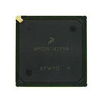
MPC561MZP56 Freescale, MPC561MZP56 Datasheet - Page 377

MPC561MZP56
Manufacturer Part Number
MPC561MZP56
Description
Manufacturer
Freescale
Datasheet
1.MPC561MZP56.pdf
(1420 pages)
Specifications of MPC561MZP56
Cpu Family
MPC56x
Device Core
PowerPC
Device Core Size
32b
Frequency (max)
56MHz
Interface Type
QSPI/SCI/SPI/UART
Total Internal Ram Size
32KB
# I/os (max)
56
Number Of Timers - General Purpose
22
Operating Supply Voltage (typ)
2.6/5V
Operating Supply Voltage (max)
2.7/5.25V
Operating Supply Voltage (min)
2.5/4.75V
On-chip Adc
2(32-chx10-bit)
Instruction Set Architecture
RISC
Operating Temp Range
-40C to 125C
Operating Temperature Classification
Automotive
Mounting
Surface Mount
Pin Count
388
Package Type
BGA
Program Memory Type
ROMLess
Program Memory Size
Not Required
Lead Free Status / RoHS Status
Not Compliant
Available stocks
Company
Part Number
Manufacturer
Quantity
Price
Company:
Part Number:
MPC561MZP56
Manufacturer:
Freescale Semiconductor
Quantity:
10 000
Company:
Part Number:
MPC561MZP56R2
Manufacturer:
Freescale Semiconductor
Quantity:
10 000
- Current page: 377 of 1420
- Download datasheet (11Mb)
9.5.8
Address transfer phase signals include the following:
Transfer attributes signals include RD/WR, BURST, TSIZ[0:1], AT[0:3], STS, and BDIP. With the
exception of the BDIP, these signals are available at the same time as the address bus.
9.5.8.1
This signal (TS) indicates the beginning of a transaction on the bus addressing a slave device. This signal
should be asserted by a master only after the ownership of the bus was granted by the arbitration protocol.
This signal is asserted for the first cycle of the transaction only and is negated in successive clock cycles
until the end of the transaction. The master should three-state this signal when it relinquishes the bus to
avoid contention between two or more masters in this line. This situation indicates that an external pull-up
resistor should be connected to the TS signal to avoid having a slave recognize this signal as asserted when
no master drives it. Refer to
9.5.8.2
The address bus consists of 32 bits, with ADDR0 the most significant bit and ADDR31 the least significant
bit. Only 24 bits (ADDR[8:31]) are available external to the MPC561/MPC563. The bus is
byte-addressable, so each address can address one or more bytes. The address and its attributes are driven
on the bus with the transfer start signal and kept valid until the bus master receives the transfer
acknowledge signal from the slave. To distinguish the individual byte, the slave device must observe the
TSIZ signals.
9.5.8.3
A high value on the RD/WR line indicates a read access. A low value indicates a write access.
9.5.8.4
BURST is driven by the bus master at the beginning of the bus cycle along with the address to indicate that
the transfer is a burst transfer.
The MPC561/MPC563 supports a non-wrapping, 8-beat maximum (with 32-bit port), critical word first
burst type. The maximum burst size is 32 bytes. For a 16-bit port, the burst includes 16 beats. For an 8-bit
port, the burst includes 32 beats at most.
The actual size of the burst is determined by the address of the starting word of the burst. Refer to
and
Freescale Semiconductor
•
•
•
Table
Transfer start
Address bus
Transfer attributes
9-6.
Address Transfer Phase Signals
Transfer Start
Address Bus
Read/Write
Burst Indicator
8- and 16-bit ports must be controlled by the memory controller.
Figure
MPC561/MPC563 Reference Manual, Rev. 1.2
9-25.
NOTE
External Bus Interface
Table 9-5
9-37
Related parts for MPC561MZP56
Image
Part Number
Description
Manufacturer
Datasheet
Request
R

Part Number:
Description:
MPC5 1K0 5%
Manufacturer:
TE Connectivity
Datasheet:

Part Number:
Description:
MPC5 500R 5%
Manufacturer:
TE Connectivity
Datasheet:

Part Number:
Description:
MPC5 5K0 5%
Manufacturer:
Tyco Electronics
Datasheet:

Part Number:
Description:
MPC5 5R0 5%
Manufacturer:
Tyco Electronics
Datasheet:

Part Number:
Description:
MPC5 50K 5%
Manufacturer:
Tyco Electronics
Datasheet:

Part Number:
Description:
MPC5 1R0 5%
Manufacturer:
Tyco Electronics
Datasheet:

Part Number:
Description:
TOWER ELEVATOR BOARDS HARDWARE
Manufacturer:
Freescale Semiconductor
Datasheet:

Part Number:
Description:
TOWER SERIAL I/O HARDWARE
Manufacturer:
Freescale Semiconductor
Datasheet:

Part Number:
Description:
LCD MODULE FOR TWR SYSTEM
Manufacturer:
Freescale Semiconductor
Datasheet:

Part Number:
Description:
DAUGHTER LCD WVGA I.MX51
Manufacturer:
Freescale Semiconductor
Datasheet:

Part Number:
Description:
TOWER SYSTEM BOARD MPC5125
Manufacturer:
Freescale Semiconductor
Datasheet:


