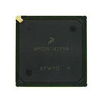
MPC561MZP56 Freescale, MPC561MZP56 Datasheet - Page 949

MPC561MZP56
Manufacturer Part Number
MPC561MZP56
Description
Manufacturer
Freescale
Datasheet
1.MPC561MZP56.pdf
(1420 pages)
Specifications of MPC561MZP56
Cpu Family
MPC56x
Device Core
PowerPC
Device Core Size
32b
Frequency (max)
56MHz
Interface Type
QSPI/SCI/SPI/UART
Total Internal Ram Size
32KB
# I/os (max)
56
Number Of Timers - General Purpose
22
Operating Supply Voltage (typ)
2.6/5V
Operating Supply Voltage (max)
2.7/5.25V
Operating Supply Voltage (min)
2.5/4.75V
On-chip Adc
2(32-chx10-bit)
Instruction Set Architecture
RISC
Operating Temp Range
-40C to 125C
Operating Temperature Classification
Automotive
Mounting
Surface Mount
Pin Count
388
Package Type
BGA
Program Memory Type
ROMLess
Program Memory Size
Not Required
Lead Free Status / RoHS Status
Not Compliant
Available stocks
Company
Part Number
Manufacturer
Quantity
Price
Company:
Part Number:
MPC561MZP56
Manufacturer:
Freescale Semiconductor
Quantity:
10 000
Company:
Part Number:
MPC561MZP56R2
Manufacturer:
Freescale Semiconductor
Quantity:
10 000
- Current page: 949 of 1420
- Download datasheet (11Mb)
When not in debug mode the sequencing error encoding indicates that the transmission from the external
development tool was a debug mode transmission. When a sequencing error occurs the development port
will ignore the data shifted in while the sequencing error was shifting out. It will be treated as a NOP
function.
Finally, the null output encoding is used to indicate that the previous transmission did not have any
associated errors.
When not in debug mode, ready will be asserted at the end of each transmission. If debug mode is not
enabled and transmission errors can be guaranteed not to occur, the status output is not needed.
23.4.6.8
When in debug mode the development port starts communications by setting DSDO low to indicate that
the CPU is trying to read an instruction from DPIR or data from DPDR. When the CPU writes data to the
port to be shifted out the ready bit is not set. The port waits for the CPU to read the next instruction before
asserting ready. This allows duplex operation of the serial port while allowing the port to control all
transmissions from the external development tool. After detecting this ready status the external
development tool begins the transmission to the development port with a start bit (logic high) on the DSDI
pin.
23.4.6.9
mode/status bit, a control/status bit, and 32 bits of data. All instructions and data for the CPU are
transmitted with the mode bit cleared indicating a 32-bit data field. The encoding of data shifted into the
development port shift register (through the DSDI pin) is shown below in
Freescale Semiconductor
In debug mode the 35 bits of the development port shift register are interpreted as a start/ready bit, a
1
2
Ready
The “Freeze” status is set to (1) when the CPU is in debug mode and to (0) otherwise.
The “Download Procedure in progress” status is asserted (0) when Debug port in the Download procedure and is
negated (1) otherwise.
(0)
(0)
(0)
(0)
Development Port Serial Communications — Debug Mode
Serial Data Into Development Port
Table 23-12. Status / Data Shifted Out of Development Port Shift Register
0
0
1
1
Status [0:1]
0
1
0
1
MPC561/MPC563 Reference Manual, Rev. 1.2
Freeze
status
Bit 0
1
Procedure
Download
progress
Bit 1
in
2
Data
Data
(Depending on Input Mode)
Bits 2:31 or 2:6 —
1’s
1’s
1’s
Table
23-13.
Valid Data from CPU
Sequencing Error
CPU Interrupt
Null
Function
Development Support
23-35
Related parts for MPC561MZP56
Image
Part Number
Description
Manufacturer
Datasheet
Request
R

Part Number:
Description:
MPC5 1K0 5%
Manufacturer:
TE Connectivity
Datasheet:

Part Number:
Description:
MPC5 500R 5%
Manufacturer:
TE Connectivity
Datasheet:

Part Number:
Description:
MPC5 5K0 5%
Manufacturer:
Tyco Electronics
Datasheet:

Part Number:
Description:
MPC5 5R0 5%
Manufacturer:
Tyco Electronics
Datasheet:

Part Number:
Description:
MPC5 50K 5%
Manufacturer:
Tyco Electronics
Datasheet:

Part Number:
Description:
MPC5 1R0 5%
Manufacturer:
Tyco Electronics
Datasheet:

Part Number:
Description:
TOWER ELEVATOR BOARDS HARDWARE
Manufacturer:
Freescale Semiconductor
Datasheet:

Part Number:
Description:
TOWER SERIAL I/O HARDWARE
Manufacturer:
Freescale Semiconductor
Datasheet:

Part Number:
Description:
LCD MODULE FOR TWR SYSTEM
Manufacturer:
Freescale Semiconductor
Datasheet:

Part Number:
Description:
DAUGHTER LCD WVGA I.MX51
Manufacturer:
Freescale Semiconductor
Datasheet:

Part Number:
Description:
TOWER SYSTEM BOARD MPC5125
Manufacturer:
Freescale Semiconductor
Datasheet:


