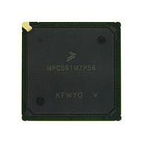
MPC561MZP56 Freescale, MPC561MZP56 Datasheet - Page 658

MPC561MZP56
Manufacturer Part Number
MPC561MZP56
Description
Manufacturer
Freescale
Datasheet
1.MPC561MZP56.pdf
(1420 pages)
Specifications of MPC561MZP56
Cpu Family
MPC56x
Device Core
PowerPC
Device Core Size
32b
Frequency (max)
56MHz
Interface Type
QSPI/SCI/SPI/UART
Total Internal Ram Size
32KB
# I/os (max)
56
Number Of Timers - General Purpose
22
Operating Supply Voltage (typ)
2.6/5V
Operating Supply Voltage (max)
2.7/5.25V
Operating Supply Voltage (min)
2.5/4.75V
On-chip Adc
2(32-chx10-bit)
Instruction Set Architecture
RISC
Operating Temp Range
-40C to 125C
Operating Temperature Classification
Automotive
Mounting
Surface Mount
Pin Count
388
Package Type
BGA
Program Memory Type
ROMLess
Program Memory Size
Not Required
Lead Free Status / RoHS Status
Not Compliant
Available stocks
Company
Part Number
Manufacturer
Quantity
Price
Company:
Part Number:
MPC561MZP56
Manufacturer:
Freescale Semiconductor
Quantity:
10 000
Company:
Part Number:
MPC561MZP56R2
Manufacturer:
Freescale Semiconductor
Quantity:
10 000
- Current page: 658 of 1420
- Download datasheet (11Mb)
Queued Serial Multi-Channel Module
When the QSPI reaches the end of the queue, it sets the SPIF flag. If the SPIFIE bit in SPCR2 is set, an
interrupt request is generated when SPIF is asserted. At this point, the QSPI clears SPE and stops unless
wraparound mode is enabled.
Slave wraparound mode is enabled by setting the WREN bit in SPCR2. The queue can wrap to pointer
address 0x0 or to the address pointed to by NEWQP, depending on the state of the WRTO bit in SPCR2.
Slave wraparound operation is identical to master wraparound operation.
15.6.6.1
Description of Slave Operation
After reset, the QSMCM registers and the QSPI control registers must be initialized as described above.
Although the command control segment is not used, the transmit and receive data segments may,
depending upon the application, need to be initialized. If meaningful data is to be sent out from the QSPI,
the data to the transmit data should be written to the segment before enabling the QSPI.
If SPE is set and MSTR is not set, a low state on the slave select (PCS0/SS) pin commences slave mode
operation at the address indicated by NEWQP. The QSPI transmits the data found in the transmit data
segment at the address indicated by NEWQP, and the QSPI stores received data in the receive data segment
at the ad-dress indicated by NEWQP. Data is transferred in response to an external slave clock input at the
SCK pin.
Because the command control segment is not used, the command control bits and peripheral chip-select
codes have no effect in slave mode operation. The QSPI does not drive any of the four peripheral
chip-selects as outputs. PCS0/SS is used as an input.
Although CONT cannot be used in slave mode, a provision is made to enable receipt of more than 16 data
bits. While keeping the QSPI selected (PCS0/SS is held low), the QSPI stores the number of bits,
designated by BITS, in the current receive data segment address, increments NEWQP, and continues
storing the remaining bits (up to the BITS value) in the next receive data segment address.
As long as PCS0/SS remains low, the QSPI continues to store the incoming bit stream in sequential receive
data segment addresses, until either the value in BITS is reached or the end-of-queue address is used with
wraparound mode disabled.
When the end of the queue is reached, the SPIF flag is asserted, optionally causing an interrupt. If
wraparound mode is disabled, any additional incoming bits are ignored.
If wraparound mode is enabled, storing continues at either address 0x0 or the address of NEWQP,
depending on the WRTO value. When using this capability to receive a long incoming data stream, the
proper delay between transfers must be used. The QSPI requires time, approximately 0.425 µs with a
40-MHz IMB3 clock, to prefetch the next transmit RAM entry for the next transfer. Therefore, a baud rate
may selected that provides at least a 0.6-µs delay between successive transfers to ensure no loss of
incoming data. If the IMB3 clock is operating at a slower rate, the delay between transfers must be
increased proportionately.
Because the BITSE option in the command control segment is no longer available, BITS sets the number
of bits to be transferred for all transfers in the queue until the CPU changes the BITS value. As mentioned
above, until PCS0/SS is negated (brought high), the QSPI continues to shift one bit for each pulse of SCK.
If PCS0/SS is negated before the proper number of bits (according to BITS) is received, the next time the
MPC561/MPC563 Reference Manual, Rev. 1.2
15-40
Freescale Semiconductor
Related parts for MPC561MZP56
Image
Part Number
Description
Manufacturer
Datasheet
Request
R

Part Number:
Description:
MPC5 1K0 5%
Manufacturer:
TE Connectivity
Datasheet:

Part Number:
Description:
MPC5 500R 5%
Manufacturer:
TE Connectivity
Datasheet:

Part Number:
Description:
MPC5 5K0 5%
Manufacturer:
Tyco Electronics
Datasheet:

Part Number:
Description:
MPC5 5R0 5%
Manufacturer:
Tyco Electronics
Datasheet:

Part Number:
Description:
MPC5 50K 5%
Manufacturer:
Tyco Electronics
Datasheet:

Part Number:
Description:
MPC5 1R0 5%
Manufacturer:
Tyco Electronics
Datasheet:

Part Number:
Description:
TOWER ELEVATOR BOARDS HARDWARE
Manufacturer:
Freescale Semiconductor
Datasheet:

Part Number:
Description:
TOWER SERIAL I/O HARDWARE
Manufacturer:
Freescale Semiconductor
Datasheet:

Part Number:
Description:
LCD MODULE FOR TWR SYSTEM
Manufacturer:
Freescale Semiconductor
Datasheet:

Part Number:
Description:
DAUGHTER LCD WVGA I.MX51
Manufacturer:
Freescale Semiconductor
Datasheet:

Part Number:
Description:
TOWER SYSTEM BOARD MPC5125
Manufacturer:
Freescale Semiconductor
Datasheet:


