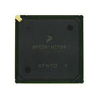
MPC561MZP56 Freescale, MPC561MZP56 Datasheet - Page 890

MPC561MZP56
Manufacturer Part Number
MPC561MZP56
Description
Manufacturer
Freescale
Datasheet
1.MPC561MZP56.pdf
(1420 pages)
Specifications of MPC561MZP56
Cpu Family
MPC56x
Device Core
PowerPC
Device Core Size
32b
Frequency (max)
56MHz
Interface Type
QSPI/SCI/SPI/UART
Total Internal Ram Size
32KB
# I/os (max)
56
Number Of Timers - General Purpose
22
Operating Supply Voltage (typ)
2.6/5V
Operating Supply Voltage (max)
2.7/5.25V
Operating Supply Voltage (min)
2.5/4.75V
On-chip Adc
2(32-chx10-bit)
Instruction Set Architecture
RISC
Operating Temp Range
-40C to 125C
Operating Temperature Classification
Automotive
Mounting
Surface Mount
Pin Count
388
Package Type
BGA
Program Memory Type
ROMLess
Program Memory Size
Not Required
Lead Free Status / RoHS Status
Not Compliant
Available stocks
Company
Part Number
Manufacturer
Quantity
Price
Company:
Part Number:
MPC561MZP56
Manufacturer:
Freescale Semiconductor
Quantity:
10 000
Company:
Part Number:
MPC561MZP56R2
Manufacturer:
Freescale Semiconductor
Quantity:
10 000
- Current page: 890 of 1420
- Download datasheet (11Mb)
CDR3 Flash (UC3F) EEPROM
21.3.8.2
The shadow information words are erased with either the lowest numbered block or small block 0,
depending on the array configuration and the state of SBEN[0]. If the lowest numbered block in the array
does not host a small block, then the shadow information words are erased with the lowest numbered
block. If the lowest numbered block hosts a small block, then the shadow information words may get
erased with small block 0. If SBEN[0] = 0 for this array configuration, then the shadow information words
get erased with the lowest numbered block. If SBEN[0] = 1 for this same array configuration, then the
shadow information words get erased with small block 0 only.
21.3.8.3
The erase operation may be suspended to allow read accesses to the array. Setting the HSUS bit in the
UC3FCTL to a 1 while EHV=1 and HVS=1 forces the array into an erase suspend state. The deassertion
of the HVS bit (HVS = 0) signifies that the erase operation has been successfully suspended. The HVS bit
should negate within 10 ms of asserting the HSUS bit.
While in erase suspend mode, normal read accesses may be performed to the UC3F array or shadow
information words. Reads to the array block or blocks targeted for erase return indeterminate data since
only a partial erase operation has been performed.
The erase operation may be resumed by setting HSUS = 0.
21.3.9
The UC3F EEPROM goes into a low power operation, or stop operation, while STOP = 1. When the STOP
bit is set, only the control registers can be accessed on the UC3F EEPROM module. The UC3F EEPROM
array may not be programmed, erased or read while STOP = 1.
21-28
State
S5
Stop Operation
Erase Suspend Operation:
The erase operation is suspended to either read
the array or disable the module. Once HVS reads
as a 0, the erase operation is suspended. Normal
reads to the array can be performed if the module
is enabled; read accesses to locations in blocks
being erased return indeterminate data.
Erasing Shadow Information Words
Erase Suspend
Repeated suspending of an erase operation to fetch array contents may
severely extend the erase operation. The internal erase hardware may only
resume the erase operation at predefined steps of the internal erase hardware
sequence; interrupting the erase operation on a high frequency basis may
cause the internal erase hardware to delay completion of the current step and
delay advancement to the next step of the internal erase hardware sequence.
Table 21-8. Erase Interlock State Descriptions (continued)
Mode
MPC561/MPC563 Reference Manual, Rev. 1.2
NOTE
State
Next
S1
S4
T10
T9
Reset.
Write HSUS = 0 or re-enable the
UC3F module.
Transition Requirement
Freescale Semiconductor
Related parts for MPC561MZP56
Image
Part Number
Description
Manufacturer
Datasheet
Request
R

Part Number:
Description:
MPC5 1K0 5%
Manufacturer:
TE Connectivity
Datasheet:

Part Number:
Description:
MPC5 500R 5%
Manufacturer:
TE Connectivity
Datasheet:

Part Number:
Description:
MPC5 5K0 5%
Manufacturer:
Tyco Electronics
Datasheet:

Part Number:
Description:
MPC5 5R0 5%
Manufacturer:
Tyco Electronics
Datasheet:

Part Number:
Description:
MPC5 50K 5%
Manufacturer:
Tyco Electronics
Datasheet:

Part Number:
Description:
MPC5 1R0 5%
Manufacturer:
Tyco Electronics
Datasheet:

Part Number:
Description:
TOWER ELEVATOR BOARDS HARDWARE
Manufacturer:
Freescale Semiconductor
Datasheet:

Part Number:
Description:
TOWER SERIAL I/O HARDWARE
Manufacturer:
Freescale Semiconductor
Datasheet:

Part Number:
Description:
LCD MODULE FOR TWR SYSTEM
Manufacturer:
Freescale Semiconductor
Datasheet:

Part Number:
Description:
DAUGHTER LCD WVGA I.MX51
Manufacturer:
Freescale Semiconductor
Datasheet:

Part Number:
Description:
TOWER SYSTEM BOARD MPC5125
Manufacturer:
Freescale Semiconductor
Datasheet:


