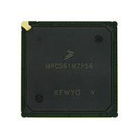
MPC561MZP56 Freescale, MPC561MZP56 Datasheet - Page 142

MPC561MZP56
Manufacturer Part Number
MPC561MZP56
Description
Manufacturer
Freescale
Datasheet
1.MPC561MZP56.pdf
(1420 pages)
Specifications of MPC561MZP56
Cpu Family
MPC56x
Device Core
PowerPC
Device Core Size
32b
Frequency (max)
56MHz
Interface Type
QSPI/SCI/SPI/UART
Total Internal Ram Size
32KB
# I/os (max)
56
Number Of Timers - General Purpose
22
Operating Supply Voltage (typ)
2.6/5V
Operating Supply Voltage (max)
2.7/5.25V
Operating Supply Voltage (min)
2.5/4.75V
On-chip Adc
2(32-chx10-bit)
Instruction Set Architecture
RISC
Operating Temp Range
-40C to 125C
Operating Temperature Classification
Automotive
Mounting
Surface Mount
Pin Count
388
Package Type
BGA
Program Memory Type
ROMLess
Program Memory Size
Not Required
Lead Free Status / RoHS Status
Not Compliant
Available stocks
Company
Part Number
Manufacturer
Quantity
Price
Company:
Part Number:
MPC561MZP56
Manufacturer:
Freescale Semiconductor
Quantity:
10 000
Company:
Part Number:
MPC561MZP56R2
Manufacturer:
Freescale Semiconductor
Quantity:
10 000
- Current page: 142 of 1420
- Download datasheet (11Mb)
Signal Descriptions
2-44
1
2
3
4
5
6
7
8
9
10
11
IRAMSTBY
Signal List
This column contains only the list of signals and should not be confused with the actual pin name. For actual pin
names, see
For 5-V outputs, the left hand value represents slew rate control off, and the right hand value represents slew rate
control on. For 2.6-V outputs, the left hand value represents loads that are full drive, and the right hand value
represents loads that are half drive.
Care should be taken that neither a pull-up to greater than 3.1 V or an external output that can drive greater than
3.1 V is connected to this pin while the 2.6-V driver is enabled.
Pull-up/pull-down is active when pin is defined as an input and/or during reset, therefore, output enable is negated.
This also means that external pull-up/pull-down is NOT required unless specified.
For this 5-V output, a drive load of 200 pf is possible but with a rise/fall time of 300 ns.
During reset, the output enable to the pad driver is negated and the PD is active. After reset is negated, the PD is
disabled.
2.6-V outputs cannot be connected to a pull-up or driver greater than 3.1 V.
This pin requires a pull-up to 2.6 V if interrupts are ever enabled for this IRQ input.
This signal also includes the MDO5 function on the K27S mask set of the MPC561.
The MODCK[1:3] are shared functions with IRQ[5:7]. If IRQ[5:7] are used as interrupts, the interrupt source should
be removed during PORESET/TRST to insure the MODCK pins are in the correct state on the rising edge of
PORESET/TRST.
These pins are powered by KAPWR (keep-alive power supply). Any pull-ups on these pins should pull-up to
KAPWR.
KAPWR
VDDSYN
VSSSYN
ALTREF
NVDDL
QVDDL
VDDH
VDDA
VSSA
VDD
VRH
VSS
VRL
11
19
1
Appendix F, “Electrical
Voltage
≥2.6 V
2.6 V
2.6 V
2.6 V
2.6 V
2.6 V
2.6 V
0 V
5 V
5 V
0 V
5 V
5 V
0 V
Table 2-14. MPC561/MPC563 Signal Reset State (continued)
Controlled
Slew Rate
Option?
MPC561/MPC563 Reference Manual, Rev. 1.2
—
—
—
—
—
—
—
—
—
—
—
—
—
—
Characteristics.”
QADC64E Power Supplies
Drive
Load
(pF)
Global Power Supplies
USIU Power Supplies
—
—
—
—
—
—
—
—
—
—
—
—
—
—
2
Reset State
—
—
—
—
—
—
—
—
—
—
—
—
—
—
Hysteresi
Enabled?
—
—
—
—
—
—
—
—
—
—
—
—
—
—
s
NVDDL
VDDH
VDDI
VSS
KAPWR
IRAMSTBY
QVDDL
VDDSYN
VSSSYN
VRH
VRL
ALTREF
VDDA
VSSA
Function After HRESET,
PORESET/TRST
Freescale Semiconductor
Related parts for MPC561MZP56
Image
Part Number
Description
Manufacturer
Datasheet
Request
R

Part Number:
Description:
MPC5 1K0 5%
Manufacturer:
TE Connectivity
Datasheet:

Part Number:
Description:
MPC5 500R 5%
Manufacturer:
TE Connectivity
Datasheet:

Part Number:
Description:
MPC5 5K0 5%
Manufacturer:
Tyco Electronics
Datasheet:

Part Number:
Description:
MPC5 5R0 5%
Manufacturer:
Tyco Electronics
Datasheet:

Part Number:
Description:
MPC5 50K 5%
Manufacturer:
Tyco Electronics
Datasheet:

Part Number:
Description:
MPC5 1R0 5%
Manufacturer:
Tyco Electronics
Datasheet:

Part Number:
Description:
TOWER ELEVATOR BOARDS HARDWARE
Manufacturer:
Freescale Semiconductor
Datasheet:

Part Number:
Description:
TOWER SERIAL I/O HARDWARE
Manufacturer:
Freescale Semiconductor
Datasheet:

Part Number:
Description:
LCD MODULE FOR TWR SYSTEM
Manufacturer:
Freescale Semiconductor
Datasheet:

Part Number:
Description:
DAUGHTER LCD WVGA I.MX51
Manufacturer:
Freescale Semiconductor
Datasheet:

Part Number:
Description:
TOWER SYSTEM BOARD MPC5125
Manufacturer:
Freescale Semiconductor
Datasheet:


