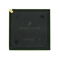
MPC561MZP56 Freescale, MPC561MZP56 Datasheet - Page 938

MPC561MZP56
Manufacturer Part Number
MPC561MZP56
Description
Manufacturer
Freescale
Datasheet
1.MPC561MZP56.pdf
(1420 pages)
Specifications of MPC561MZP56
Cpu Family
MPC56x
Device Core
PowerPC
Device Core Size
32b
Frequency (max)
56MHz
Interface Type
QSPI/SCI/SPI/UART
Total Internal Ram Size
32KB
# I/os (max)
56
Number Of Timers - General Purpose
22
Operating Supply Voltage (typ)
2.6/5V
Operating Supply Voltage (max)
2.7/5.25V
Operating Supply Voltage (min)
2.5/4.75V
On-chip Adc
2(32-chx10-bit)
Instruction Set Architecture
RISC
Operating Temp Range
-40C to 125C
Operating Temperature Classification
Automotive
Mounting
Surface Mount
Pin Count
388
Package Type
BGA
Program Memory Type
ROMLess
Program Memory Size
Not Required
Lead Free Status / RoHS Status
Not Compliant
Available stocks
Company
Part Number
Manufacturer
Quantity
Price
Company:
Part Number:
MPC561MZP56
Manufacturer:
Freescale Semiconductor
Quantity:
10 000
Company:
Part Number:
MPC561MZP56R2
Manufacturer:
Freescale Semiconductor
Quantity:
10 000
- Current page: 938 of 1420
- Download datasheet (11Mb)
Development Support
The debug interface is enabled by:
or
The state of this pin is sampled three clocks before the negation of SRESET.
If the DSCK pin is sampled negated, debug mode is disabled until a subsequent reset when the DSCK pin
is sampled in the asserted state. When debug mode is disabled the internal watchpoint/breakpoint hardware
will still be operational and may be used by a software monitor program for debugging purposes.
When debug mode is disabled, all development support registers (see list in
the supervisor code (MSR[PR] = 0) and can be used by a monitor debugger software. However, the
processor never enters debug mode and, therefore, the exception cause register (ECR) and the debug
enable register (DER) are used only for asserting and negating the freeze signal. For more information on
the software monitor debugger support refer to
When debug mode is enabled, all development support registers are accessible only when the CPU is in
debug mode. Therefore, even supervisor code that may be still under debug cannot prevent the CPU from
entering debug mode. The development system has full control of all development support features of the
CPU through the development port. Refer to
23.3.1.2
Entering debug mode can be a result of a number of events. All events have a programmable enable bit to
selectively decide which events result in debug mode entry and which in regular interrupt handling.
23-24
•
•
JCOMP/RSTI
PORESET
Configuration
holding JCOMP/RSTI low while HRESET is asserted and then entering BDM (DSCK=high at
HRESET negation)
configuring READI to be disabled (EVTI=high at RSTI negation) and then entering BDM
(DSCK=high at HRESET negation)
Entering Debug Mode
Because SRESET negation is done by an external pull up resistor any
reference here to SRESET negation time refers to the time the
MPC561/MPC563 releases SRESET. If the actual negation is slow due to a
large resistor, set up time for the debug port signals should be set
accordingly.
(Low)
JTAG disabled
MPC561/MPC563 Reference Manual, Rev. 1.2
Figure 23-7. BDM Mode Selection
Table
READI Disabled/ BDM can be enabled/entered
Section 23.5, “Software Monitor Debugger
NOTE
23-16.
Table
23-14) are accessible to
Freescale Semiconductor
T
Support.”
Related parts for MPC561MZP56
Image
Part Number
Description
Manufacturer
Datasheet
Request
R

Part Number:
Description:
MPC5 1K0 5%
Manufacturer:
TE Connectivity
Datasheet:

Part Number:
Description:
MPC5 500R 5%
Manufacturer:
TE Connectivity
Datasheet:

Part Number:
Description:
MPC5 5K0 5%
Manufacturer:
Tyco Electronics
Datasheet:

Part Number:
Description:
MPC5 5R0 5%
Manufacturer:
Tyco Electronics
Datasheet:

Part Number:
Description:
MPC5 50K 5%
Manufacturer:
Tyco Electronics
Datasheet:

Part Number:
Description:
MPC5 1R0 5%
Manufacturer:
Tyco Electronics
Datasheet:

Part Number:
Description:
TOWER ELEVATOR BOARDS HARDWARE
Manufacturer:
Freescale Semiconductor
Datasheet:

Part Number:
Description:
TOWER SERIAL I/O HARDWARE
Manufacturer:
Freescale Semiconductor
Datasheet:

Part Number:
Description:
LCD MODULE FOR TWR SYSTEM
Manufacturer:
Freescale Semiconductor
Datasheet:

Part Number:
Description:
DAUGHTER LCD WVGA I.MX51
Manufacturer:
Freescale Semiconductor
Datasheet:

Part Number:
Description:
TOWER SYSTEM BOARD MPC5125
Manufacturer:
Freescale Semiconductor
Datasheet:


