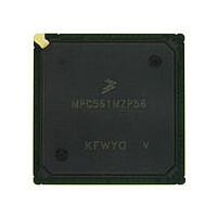
MPC561MZP56 Freescale, MPC561MZP56 Datasheet - Page 1371

MPC561MZP56
Manufacturer Part Number
MPC561MZP56
Description
Manufacturer
Freescale
Datasheet
1.MPC561MZP56.pdf
(1420 pages)
Specifications of MPC561MZP56
Cpu Family
MPC56x
Device Core
PowerPC
Device Core Size
32b
Frequency (max)
56MHz
Interface Type
QSPI/SCI/SPI/UART
Total Internal Ram Size
32KB
# I/os (max)
56
Number Of Timers - General Purpose
22
Operating Supply Voltage (typ)
2.6/5V
Operating Supply Voltage (max)
2.7/5.25V
Operating Supply Voltage (min)
2.5/4.75V
On-chip Adc
2(32-chx10-bit)
Instruction Set Architecture
RISC
Operating Temp Range
-40C to 125C
Operating Temperature Classification
Automotive
Mounting
Surface Mount
Pin Count
388
Package Type
BGA
Program Memory Type
ROMLess
Program Memory Size
Not Required
Lead Free Status / RoHS Status
Not Compliant
Available stocks
Company
Part Number
Manufacturer
Quantity
Price
Company:
Part Number:
MPC561MZP56
Manufacturer:
Freescale Semiconductor
Quantity:
10 000
Company:
Part Number:
MPC561MZP56R2
Manufacturer:
Freescale Semiconductor
Quantity:
10 000
- Current page: 1371 of 1420
- Download datasheet (11Mb)
Note: All delays are in system clock periods.
Freescale Semiconductor
1
2
3
MDASM pin high time
Input capture resolution
Input pin to Counter Bus capture delay
Input pin to interrupt flag delay
Input pin to PIN delay
Counter bus resolution
Output pulse width
Compare resolution
Counter Bus to pin change
Counter Bus to interrupt flag set.
If the counter bus capture occurs when the counter bus is changing then the capture is delayed one cycle. In
situations where the counter bus is stable when the input capture occurs the t
cycles (the one-cycle uncertainty is due to the synchronizer).
Maximum resolution is obtained by setting CPSMPSL[3:0] =0x2 and MDASMSCR_CP[7:0] =0xFF.
Maximum output resolution and pulse width depends on counter (e.g., MMCSM) and MCPSM prescaler
settings.
MDAI input pin
f
SYS
Characteristics
f
SYS
is the internal system clock for the IMB3 bus.
3
3
Figure G-56. MDASM Minimum Input Pin Timing Diagram
Table G-26. MDASM Timing Characteristics (continued)
MPC561/MPC563 Reference Manual, Rev. 1.2
Output Modes: (OC, OPWM)
t
PPER
min
Symbol
t
NOTE
t
t
t
t
t
CBFLG
COMR
t
PULW
CAPR
PCAP
t
PFLG
t
t
CBR
CBP
PHI
PIN
t
min
PLO
Min
—
—
—
2
1
2
1
2
PCAP
t
min
PHI
has a maximum delay of two
3
3
66-MHz Electrical Characteristics
Max
—
3
2
—
2
2
3
2
1
2
2
G-65
Related parts for MPC561MZP56
Image
Part Number
Description
Manufacturer
Datasheet
Request
R

Part Number:
Description:
MPC5 1K0 5%
Manufacturer:
TE Connectivity
Datasheet:

Part Number:
Description:
MPC5 500R 5%
Manufacturer:
TE Connectivity
Datasheet:

Part Number:
Description:
MPC5 5K0 5%
Manufacturer:
Tyco Electronics
Datasheet:

Part Number:
Description:
MPC5 5R0 5%
Manufacturer:
Tyco Electronics
Datasheet:

Part Number:
Description:
MPC5 50K 5%
Manufacturer:
Tyco Electronics
Datasheet:

Part Number:
Description:
MPC5 1R0 5%
Manufacturer:
Tyco Electronics
Datasheet:

Part Number:
Description:
TOWER ELEVATOR BOARDS HARDWARE
Manufacturer:
Freescale Semiconductor
Datasheet:

Part Number:
Description:
TOWER SERIAL I/O HARDWARE
Manufacturer:
Freescale Semiconductor
Datasheet:

Part Number:
Description:
LCD MODULE FOR TWR SYSTEM
Manufacturer:
Freescale Semiconductor
Datasheet:

Part Number:
Description:
DAUGHTER LCD WVGA I.MX51
Manufacturer:
Freescale Semiconductor
Datasheet:

Part Number:
Description:
TOWER SYSTEM BOARD MPC5125
Manufacturer:
Freescale Semiconductor
Datasheet:


