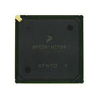
MPC561MZP56 Freescale, MPC561MZP56 Datasheet - Page 653

MPC561MZP56
Manufacturer Part Number
MPC561MZP56
Description
Manufacturer
Freescale
Datasheet
1.MPC561MZP56.pdf
(1420 pages)
Specifications of MPC561MZP56
Cpu Family
MPC56x
Device Core
PowerPC
Device Core Size
32b
Frequency (max)
56MHz
Interface Type
QSPI/SCI/SPI/UART
Total Internal Ram Size
32KB
# I/os (max)
56
Number Of Timers - General Purpose
22
Operating Supply Voltage (typ)
2.6/5V
Operating Supply Voltage (max)
2.7/5.25V
Operating Supply Voltage (min)
2.5/4.75V
On-chip Adc
2(32-chx10-bit)
Instruction Set Architecture
RISC
Operating Temp Range
-40C to 125C
Operating Temperature Classification
Automotive
Mounting
Surface Mount
Pin Count
388
Package Type
BGA
Program Memory Type
ROMLess
Program Memory Size
Not Required
Lead Free Status / RoHS Status
Not Compliant
Available stocks
Company
Part Number
Manufacturer
Quantity
Price
Company:
Part Number:
MPC561MZP56
Manufacturer:
Freescale Semiconductor
Quantity:
10 000
Company:
Part Number:
MPC561MZP56R2
Manufacturer:
Freescale Semiconductor
Quantity:
10 000
- Current page: 653 of 1420
- Download datasheet (11Mb)
When the proper number of bits have been transferred, the QSPI stores the working queue pointer value
in CPTQP, increments the working queue pointer, and loads the next data for transfer from transmit RAM.
The command pointed to by the incremented working queue pointer is executed next, unless a new value
has been written to NEWQP. If a new queue pointer value is written while a transfer is in progress, that
transfer is completed normally.
When the CONT bit in a command RAM byte is set, PCS pins are continuously driven to specified states
during and between transfers. If the chip-select pattern changes during or between transfers, the original
pattern is driven until execution of the following transfer begins. When CONT is cleared, the data in
register PORTQS is driven between transfers. The data in PORTQS must match the inactive states of SCK
and any peripheral chip-selects used.
When the QSPI reaches the end of the queue, it sets the SPIF flag. If the SPIFIE bit in SPCR2 is set, an
interrupt request is generated when SPIF is asserted. At this point, the QSPI clears SPE and stops unless
wraparound mode is enabled.
15.6.5.1
In master mode, data transfer is synchronized with the internally-generated serial clock SCK. Control bits,
CPHA and CPOL, in SPCR0, control clock phase and polarity. Combinations of CPHA and CPOL
determine upon which SCK edge to drive outgoing data from the MOSI pin and to latch incoming data
from the MISO pin.
15.6.5.2
Baud rate is selected by writing a value from two to 255 into the SPBR field in SPCR0. The QSPI uses a
modulus counter to derive the SCK baud rate from the MCU IMB3 clock.
The following expressions apply to the SCK baud rate:
Giving SPBR a value of zero or one disables the baud rate generator. SCK is disabled and assumes its
inactive state. At reset, the SCK baud rate is initialized to one eighth of the IMB3 clock frequency.
Table 15-21
Freescale Semiconductor
provides some example SCK baud rates with a 40-MHz IMB3 clock.
Clock Phase and Polarity
Baud Rate Selection
Table 15-21. Example SCK Frequencies with a 40-MHz IMB3 Clock
Division Ratio
MPC561/MPC563 Reference Manual, Rev. 1.2
SPBR
4
6
8
SCK Baud Rate
=
-----------------------------------------------------------------------
2xSCK Baud Rate Desired
SPBR Value
or
2
3
4
=
f
SYS
---------------------- -
2xSPBR
f
SYS
Frequency
10.00 MHz
6.67 MHz
5.00 MHz
SCK
Queued Serial Multi-Channel Module
Eqn. 15-1
Eqn. 15-2
15-35
Related parts for MPC561MZP56
Image
Part Number
Description
Manufacturer
Datasheet
Request
R

Part Number:
Description:
MPC5 1K0 5%
Manufacturer:
TE Connectivity
Datasheet:

Part Number:
Description:
MPC5 500R 5%
Manufacturer:
TE Connectivity
Datasheet:

Part Number:
Description:
MPC5 5K0 5%
Manufacturer:
Tyco Electronics
Datasheet:

Part Number:
Description:
MPC5 5R0 5%
Manufacturer:
Tyco Electronics
Datasheet:

Part Number:
Description:
MPC5 50K 5%
Manufacturer:
Tyco Electronics
Datasheet:

Part Number:
Description:
MPC5 1R0 5%
Manufacturer:
Tyco Electronics
Datasheet:

Part Number:
Description:
TOWER ELEVATOR BOARDS HARDWARE
Manufacturer:
Freescale Semiconductor
Datasheet:

Part Number:
Description:
TOWER SERIAL I/O HARDWARE
Manufacturer:
Freescale Semiconductor
Datasheet:

Part Number:
Description:
LCD MODULE FOR TWR SYSTEM
Manufacturer:
Freescale Semiconductor
Datasheet:

Part Number:
Description:
DAUGHTER LCD WVGA I.MX51
Manufacturer:
Freescale Semiconductor
Datasheet:

Part Number:
Description:
TOWER SYSTEM BOARD MPC5125
Manufacturer:
Freescale Semiconductor
Datasheet:


