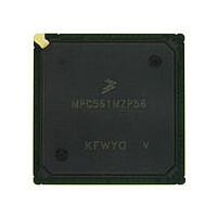
MPC561MZP56 Freescale, MPC561MZP56 Datasheet - Page 536

MPC561MZP56
Manufacturer Part Number
MPC561MZP56
Description
Manufacturer
Freescale
Datasheet
1.MPC561MZP56.pdf
(1420 pages)
Specifications of MPC561MZP56
Cpu Family
MPC56x
Device Core
PowerPC
Device Core Size
32b
Frequency (max)
56MHz
Interface Type
QSPI/SCI/SPI/UART
Total Internal Ram Size
32KB
# I/os (max)
56
Number Of Timers - General Purpose
22
Operating Supply Voltage (typ)
2.6/5V
Operating Supply Voltage (max)
2.7/5.25V
Operating Supply Voltage (min)
2.5/4.75V
On-chip Adc
2(32-chx10-bit)
Instruction Set Architecture
RISC
Operating Temp Range
-40C to 125C
Operating Temperature Classification
Automotive
Mounting
Surface Mount
Pin Count
388
Package Type
BGA
Program Memory Type
ROMLess
Program Memory Size
Not Required
Lead Free Status / RoHS Status
Not Compliant
Available stocks
Company
Part Number
Manufacturer
Quantity
Price
Company:
Part Number:
MPC561MZP56
Manufacturer:
Freescale Semiconductor
Quantity:
10 000
Company:
Part Number:
MPC561MZP56R2
Manufacturer:
Freescale Semiconductor
Quantity:
10 000
- Current page: 536 of 1420
- Download datasheet (11Mb)
QADC64E Legacy Mode Operation
Series resistance can be used with the capacitor on an input signal to implement a simple RC filter. The
maximum level of filtering at the input signals is application dependent and is based on the bandpass
characteristics required to accurately track the dynamic characteristics of an input. Simple RC filtering at
the signal may be limited by the source impedance of the transducer or circuit supplying the analog signal
to be measured. Refer to
cases, the size of the capacitor at the signal may be very small.
Figure 13-52
the interaction between the external circuitry and the circuitry inside the QADC64E.
In
C
to provide charge to C
The following paragraphs provide a simplified description of the interaction between the QADC64E and
the external circuitry. This circuitry is assumed to be a simple RC low-pass filter passing a signal from a
source to the QADC64E input signal. The following simplifying assumptions are made:
13-72
SAMP
Figure
•
•
•
•
is the capacitor array used to sample and hold the input voltage. V
It sources charge during the sample period when the analog signal source is a high-impedance
source.
The external capacitor is perfect (no leakage, no significant dielectric absorption characteristics,
etc.)
All parasitic capacitance associated with the input signal is included in the value of the external
capacitor
Inductance is ignored
V
R
C
C
R
C
V
13-52, R
F
F
P
SRC
SRC
I
SAMP
Source
= Filter Impedance
= Filter Capacitor
= Internal Voltage Source during Sample and Hold
= Internal Parasitic Capacitance
V
is a simplified model of an input channel. Refer to this model in the following discussion of
SRC
= Source Impedance
R
= Source Voltage
SRC
= Sample Capacitor
F
, R
SRC
SAMP
External Filter
Section 13.7.5.3, “Error Resulting from
and C
R F
Figure 13-52. Electrical Model of an A/D Input Signal
during sample phase.
C F
F
MPC561/MPC563 Reference Manual, Rev. 1.2
comprise the external filter circuit. C
Internal Circuit Model
S1
C P
AMP
Leakage,” for more information. In some
S2
QADC64E Sample AMP Model
P
I
is the internal parasitic capacitor.
is an internal voltage source used
C
SAMP
S3
Freescale Semiconductor
VI
Related parts for MPC561MZP56
Image
Part Number
Description
Manufacturer
Datasheet
Request
R

Part Number:
Description:
MPC5 1K0 5%
Manufacturer:
TE Connectivity
Datasheet:

Part Number:
Description:
MPC5 500R 5%
Manufacturer:
TE Connectivity
Datasheet:

Part Number:
Description:
MPC5 5K0 5%
Manufacturer:
Tyco Electronics
Datasheet:

Part Number:
Description:
MPC5 5R0 5%
Manufacturer:
Tyco Electronics
Datasheet:

Part Number:
Description:
MPC5 50K 5%
Manufacturer:
Tyco Electronics
Datasheet:

Part Number:
Description:
MPC5 1R0 5%
Manufacturer:
Tyco Electronics
Datasheet:

Part Number:
Description:
TOWER ELEVATOR BOARDS HARDWARE
Manufacturer:
Freescale Semiconductor
Datasheet:

Part Number:
Description:
TOWER SERIAL I/O HARDWARE
Manufacturer:
Freescale Semiconductor
Datasheet:

Part Number:
Description:
LCD MODULE FOR TWR SYSTEM
Manufacturer:
Freescale Semiconductor
Datasheet:

Part Number:
Description:
DAUGHTER LCD WVGA I.MX51
Manufacturer:
Freescale Semiconductor
Datasheet:

Part Number:
Description:
TOWER SYSTEM BOARD MPC5125
Manufacturer:
Freescale Semiconductor
Datasheet:


