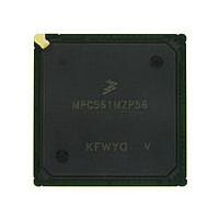
MPC561MZP56 Freescale, MPC561MZP56 Datasheet - Page 404

MPC561MZP56
Manufacturer Part Number
MPC561MZP56
Description
Manufacturer
Freescale
Datasheet
1.MPC561MZP56.pdf
(1420 pages)
Specifications of MPC561MZP56
Cpu Family
MPC56x
Device Core
PowerPC
Device Core Size
32b
Frequency (max)
56MHz
Interface Type
QSPI/SCI/SPI/UART
Total Internal Ram Size
32KB
# I/os (max)
56
Number Of Timers - General Purpose
22
Operating Supply Voltage (typ)
2.6/5V
Operating Supply Voltage (max)
2.7/5.25V
Operating Supply Voltage (min)
2.5/4.75V
On-chip Adc
2(32-chx10-bit)
Instruction Set Architecture
RISC
Operating Temp Range
-40C to 125C
Operating Temperature Classification
Automotive
Mounting
Surface Mount
Pin Count
388
Package Type
BGA
Program Memory Type
ROMLess
Program Memory Size
Not Required
Lead Free Status / RoHS Status
Not Compliant
Available stocks
Company
Part Number
Manufacturer
Quantity
Price
Company:
Part Number:
MPC561MZP56
Manufacturer:
Freescale Semiconductor
Quantity:
10 000
Company:
Part Number:
MPC561MZP56R2
Manufacturer:
Freescale Semiconductor
Quantity:
10 000
- Current page: 404 of 1420
- Download datasheet (11Mb)
Memory Controller
For addition details, refer to
10.2.6
In order to meet timing requirements when interfacing to external memories, the data setup time can be
reduced. This mode can be selected by programming the BRx registers. Thus there is flexibility in how
each region can be configured to operate. The operation mode will be determined dynamically according
to a particular access type. This means that for a memory region with the reduced setup time mode enabled,
the mode will automatically switch to disabled when there is no requirement for the reduced setup time,
(e.g., a back-to-back load/store access). For a new access with burst length more than 1, the operation
mode will be automatically switched back to the reduced setup time mode.
Reduced setup time can be selected via the SST bit in BR[0
Base Registers
access with reduced data setup time will corrupt a load/store to any USIU register.
The reduced setup time mode may or may not have a performance impact, depending on the properties of
the memory. Namely, there is always an additional empty cycle between two burst sequences. On the other
hand, this additional cycle, under certain conditions, may be compensated for by reducing the number of
cycles in initial data access and sequential burst beats.
10.2.6.1
Initial access:
To derive the number of clocks required, divide by the system clock cycle time:
Burst access:
The number of clocks required
This case is illustrated in
10-6
--------- -
17.9
56
Cycle time at 56 MHz = 17.9 ns
Short setup time = 3 ns
Normal setup time = 6 ns
Additional delay arising from on-board wires and clock skew between
internal clock and CLKOUT
Initial access time of memory
Burst access time of memory
=
3.13
Reduced Data Setup Time
Case 1: Normal Setup Time
(BR0–BR3)” for more details. If SCCR[EBDF] is greater than 0, however, an external burst
therefore 4 cycles are required
Table 10-1. Timing Requirements for Reduced Setup Time
CPU Specification
Figure
Section 9.5.4, “Burst
10-5.
MPC561/MPC563 Reference Manual, Rev. 1.2
=
+
--------- -
17.9
+
20
Data setup time of CPU
Data setup time of CPU
=
1.11
Transfer."
therefore 2 clocks are required.
:
3]. See
+
Initial access time = 49 ns
Burst access time = 13 ns
+
Delays
Delays
Section 10.9.3, “Memory Controller
Memory Device Requirements
=
=
13
49
+
+
6
6
+
+
1
1
Freescale Semiconductor
=
=
20ns
56ns
Related parts for MPC561MZP56
Image
Part Number
Description
Manufacturer
Datasheet
Request
R

Part Number:
Description:
MPC5 1K0 5%
Manufacturer:
TE Connectivity
Datasheet:

Part Number:
Description:
MPC5 500R 5%
Manufacturer:
TE Connectivity
Datasheet:

Part Number:
Description:
MPC5 5K0 5%
Manufacturer:
Tyco Electronics
Datasheet:

Part Number:
Description:
MPC5 5R0 5%
Manufacturer:
Tyco Electronics
Datasheet:

Part Number:
Description:
MPC5 50K 5%
Manufacturer:
Tyco Electronics
Datasheet:

Part Number:
Description:
MPC5 1R0 5%
Manufacturer:
Tyco Electronics
Datasheet:

Part Number:
Description:
TOWER ELEVATOR BOARDS HARDWARE
Manufacturer:
Freescale Semiconductor
Datasheet:

Part Number:
Description:
TOWER SERIAL I/O HARDWARE
Manufacturer:
Freescale Semiconductor
Datasheet:

Part Number:
Description:
LCD MODULE FOR TWR SYSTEM
Manufacturer:
Freescale Semiconductor
Datasheet:

Part Number:
Description:
DAUGHTER LCD WVGA I.MX51
Manufacturer:
Freescale Semiconductor
Datasheet:

Part Number:
Description:
TOWER SYSTEM BOARD MPC5125
Manufacturer:
Freescale Semiconductor
Datasheet:


