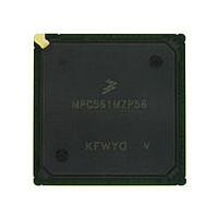
MPC561MZP56 Freescale, MPC561MZP56 Datasheet - Page 1121

MPC561MZP56
Manufacturer Part Number
MPC561MZP56
Description
Manufacturer
Freescale
Datasheet
1.MPC561MZP56.pdf
(1420 pages)
Specifications of MPC561MZP56
Cpu Family
MPC56x
Device Core
PowerPC
Device Core Size
32b
Frequency (max)
56MHz
Interface Type
QSPI/SCI/SPI/UART
Total Internal Ram Size
32KB
# I/os (max)
56
Number Of Timers - General Purpose
22
Operating Supply Voltage (typ)
2.6/5V
Operating Supply Voltage (max)
2.7/5.25V
Operating Supply Voltage (min)
2.5/4.75V
On-chip Adc
2(32-chx10-bit)
Instruction Set Architecture
RISC
Operating Temp Range
-40C to 125C
Operating Temperature Classification
Automotive
Mounting
Surface Mount
Pin Count
388
Package Type
BGA
Program Memory Type
ROMLess
Program Memory Size
Not Required
Lead Free Status / RoHS Status
Not Compliant
Available stocks
Company
Part Number
Manufacturer
Quantity
Price
Company:
Part Number:
MPC561MZP56
Manufacturer:
Freescale Semiconductor
Quantity:
10 000
Company:
Part Number:
MPC561MZP56R2
Manufacturer:
Freescale Semiconductor
Quantity:
10 000
- Current page: 1121 of 1420
- Download datasheet (11Mb)
Freescale Semiconductor
0x30 400E
0x30 4010
0x30 4012
0x30 4014
0x30 4016
0x30 4018
0x30 401A
0x30 401C
0x30 401E
0x30 4020
0x30 4022
0x30 4024
0x30 4026
0x30 4028
0x30 402A
0x30 402C
0x30 402E
0x30 4100 –
0x30 410F
0x30 4110 –
0x30 411F
0x30 4120 –
0x30 412F
0x30 4130 –
0x30 413F
0x30 4140 –
0x30 414F
Address
Access
Table B-9. Time Processor Unit 3 A and B (TPU3 A and B) (continued)
S/U3
S/U3
S/U
S/U
S/U
S/U
S/U
S/U
S/U
S
S
S
S
S
S
S
T
T
T
S
T
T
5
3
3
3
3
3
3
3
TPUMCR2_A
TPUMCR3_A
HSQR0_A
HSQR1_A
HSRR0_A
HSRR1_A
CFSR1_A
CFSR2_A
CFSR3_A
DCNR_A
CPR0_A
CPR1_A
SGLR_A
Symbol
CISR_A
ISDR_A
ISCR_A
LR_A
MPC561/MPC563 Reference Manual, Rev. 1.2
—
—
—
—
—
TPU3_A Channel Function Selection Register 1.
See <XrefBlue>Table 19-12 for bit descriptions.
TPU3_A Channel Function Selection Register 2.
See <XrefBlue>Table 19-12 for bit descriptions.
TPU3_A Channel Function Selection Register 3.
See <XrefBlue>Table 19-12 for bit descriptions.
TPU3_A Host Sequence Register 0.
See <XrefBlue>Table 19-13 for bit descriptions.
TPU3_A Host Sequence Register 1.
See <XrefBlue>Table 19-13 for bit descriptions.
TPU3_A Host Service Request Register 0.
See <XrefBlue>Table 19-14 for bit descriptions.
TPU3_A Host Service Request Register 1.
See <XrefBlue>Table 19-14 for bit descriptions.
TPU3_A Channel Priority Register 0.
See <XrefBlue>Table 19-15 for bit descriptions.
TPU3_A Channel Priority Register 1.
See <XrefBlue>Table 19-15 for bit descriptions.
TPU3_A Channel Interrupt Status Register.
See <XrefBlue>Table 19-17 for bit descriptions.
TPU3_A Link Register
TPU3_A Service Grant Latch Register
TPU3_A Decoded Channel Number Register
TPU3_A Module Configuration Register 2.
See <XrefBlue>Table 19-18 for bit descriptions.
TPU3_A Module Configuration Register 3.
See <XrefBlue>Table 19-21 for bit descriptions.
TPU3_A Internal Scan Data Register
TPU3_A Internal Scan Control Register
TPU3_A Channel 0 Parameter Registers.
See
TPU3_A Channel 1 Parameter Registers.
See
TPU3_A Channel 2 Parameter Registers.
See
TPU3_A Channel 3 Parameter Registers.
See
TPU3_A Channel 4 Parameter Registers.
See
Section 19.4.15
Section 19.4.15
Section 19.4.15
Section 19.4.15
Section 19.4.15
Register
for more information.
for more information.
for more information.
for more information.
for more information.
4
4
4
16, 32
16, 32
16, 32
16, 32
16, 32
16, 32
16, 32
Size
16
16
16
16
16
16
16
16
16
16
16
16
16
16
16
Internal Memory Map
2
2
2
2
2
2
2
2
2
2
2
2
2
2
2
2
2
2
2
2
2
Reset
S, M
S, M
S, M
S, M
S, M
S, M
S, M
S, M
S, M
S, M
S, M
S, M
S, M
S, M
S, M
—
—
—
—
—
—
—
B-11
Related parts for MPC561MZP56
Image
Part Number
Description
Manufacturer
Datasheet
Request
R

Part Number:
Description:
MPC5 1K0 5%
Manufacturer:
TE Connectivity
Datasheet:

Part Number:
Description:
MPC5 500R 5%
Manufacturer:
TE Connectivity
Datasheet:

Part Number:
Description:
MPC5 5K0 5%
Manufacturer:
Tyco Electronics
Datasheet:

Part Number:
Description:
MPC5 5R0 5%
Manufacturer:
Tyco Electronics
Datasheet:

Part Number:
Description:
MPC5 50K 5%
Manufacturer:
Tyco Electronics
Datasheet:

Part Number:
Description:
MPC5 1R0 5%
Manufacturer:
Tyco Electronics
Datasheet:

Part Number:
Description:
TOWER ELEVATOR BOARDS HARDWARE
Manufacturer:
Freescale Semiconductor
Datasheet:

Part Number:
Description:
TOWER SERIAL I/O HARDWARE
Manufacturer:
Freescale Semiconductor
Datasheet:

Part Number:
Description:
LCD MODULE FOR TWR SYSTEM
Manufacturer:
Freescale Semiconductor
Datasheet:

Part Number:
Description:
DAUGHTER LCD WVGA I.MX51
Manufacturer:
Freescale Semiconductor
Datasheet:

Part Number:
Description:
TOWER SYSTEM BOARD MPC5125
Manufacturer:
Freescale Semiconductor
Datasheet:


