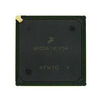
MPC561MZP56 Freescale, MPC561MZP56 Datasheet - Page 595

MPC561MZP56
Manufacturer Part Number
MPC561MZP56
Description
Manufacturer
Freescale
Datasheet
1.MPC561MZP56.pdf
(1420 pages)
Specifications of MPC561MZP56
Cpu Family
MPC56x
Device Core
PowerPC
Device Core Size
32b
Frequency (max)
56MHz
Interface Type
QSPI/SCI/SPI/UART
Total Internal Ram Size
32KB
# I/os (max)
56
Number Of Timers - General Purpose
22
Operating Supply Voltage (typ)
2.6/5V
Operating Supply Voltage (max)
2.7/5.25V
Operating Supply Voltage (min)
2.5/4.75V
On-chip Adc
2(32-chx10-bit)
Instruction Set Architecture
RISC
Operating Temp Range
-40C to 125C
Operating Temperature Classification
Automotive
Mounting
Surface Mount
Pin Count
388
Package Type
BGA
Program Memory Type
ROMLess
Program Memory Size
Not Required
Lead Free Status / RoHS Status
Not Compliant
Available stocks
Company
Part Number
Manufacturer
Quantity
Price
Company:
Part Number:
MPC561MZP56
Manufacturer:
Freescale Semiconductor
Quantity:
10 000
Company:
Part Number:
MPC561MZP56R2
Manufacturer:
Freescale Semiconductor
Quantity:
10 000
- Current page: 595 of 1420
- Download datasheet (11Mb)
32-bit accesses to an even address require two bus cycles to complete the access, and two full 16-bit
QADC64E locations are accessed. The first bus cycle reads or writes the addressed 16-bit QADC64E
location and the second cycle reads or writes the following 16-bit location.
32-bit accesses to an odd address require three bus cycles. Portions of three different QADC64E locations
are accessed. The first bus cycle is treated by the QADC64E as an 8-bit access of an odd address, the
second cycle is a 16-bit aligned access, and the third cycle is an 8-bit access of an even address. The
QADC64E address space is organized into 16-bit even address locations, so a 32-bit read or write of an
odd address provides the lower half of one QADC64E location, the full 16-bit content of the following
QADC64E location, and the upper half of the third QADC64E location.
14.5
This section contains examples describing queue priority and conversion timing schemes.
14.5.1
Since there are two conversion command queues and only one A/D converter, there is a priority scheme
to determine which conversion is to occur. Each queue has a variety of trigger events that are intended to
initiate conversions, and they can occur asynchronously in relation to each other and other conversions in
progress. For example, a queue can be idle awaiting a trigger event, a trigger event can have occurred but
the first conversion has not started, a conversion can be in progress, a pause condition can exist awaiting
another trigger event to continue the queue, and so on.
The following paragraphs and figures outline the prioritizing criteria used to determine which conversion
occurs in each overlap situation.
Trigger events are described in
Freescale Semiconductor
Trigger and Queue Interaction Examples
Queue Priority Schemes
The situations in
S19. In each diagram, time is shown increasing from left to right. The
execution of queue 1 and queue 2 (Q1 and Q2) is shown as a string of
rectangles representing the execution time of each CCW in the queue. In
most of the situations, there are four CCWs (labeled C1 to C4) in both queue
1 and queue 2. In some of the situations, CCW C2 is presumed to have the
pause bit set, to show the similarities of pause and end-of-queue as
terminations of queue execution.
Trigger
T1
T2
Table
Figure 14-25
MPC561/MPC563 Reference Manual, Rev. 1.2
Events that trigger queue 1 execution (external trigger, software
initiated single-scan enable bit, or completion of the previous
continuous loop)
Events that trigger queue 2 execution (external trigger, software
initiated single-scan enable bit, timer period/interval expired, or
completion of the previous continuous loop)
14-23.
Table 14-23. Trigger Events
through
NOTE
Figure 14-43
Events
are labeled S1 through
QADC64E Enhanced Mode Operation
14-53
Related parts for MPC561MZP56
Image
Part Number
Description
Manufacturer
Datasheet
Request
R

Part Number:
Description:
MPC5 1K0 5%
Manufacturer:
TE Connectivity
Datasheet:

Part Number:
Description:
MPC5 500R 5%
Manufacturer:
TE Connectivity
Datasheet:

Part Number:
Description:
MPC5 5K0 5%
Manufacturer:
Tyco Electronics
Datasheet:

Part Number:
Description:
MPC5 5R0 5%
Manufacturer:
Tyco Electronics
Datasheet:

Part Number:
Description:
MPC5 50K 5%
Manufacturer:
Tyco Electronics
Datasheet:

Part Number:
Description:
MPC5 1R0 5%
Manufacturer:
Tyco Electronics
Datasheet:

Part Number:
Description:
TOWER ELEVATOR BOARDS HARDWARE
Manufacturer:
Freescale Semiconductor
Datasheet:

Part Number:
Description:
TOWER SERIAL I/O HARDWARE
Manufacturer:
Freescale Semiconductor
Datasheet:

Part Number:
Description:
LCD MODULE FOR TWR SYSTEM
Manufacturer:
Freescale Semiconductor
Datasheet:

Part Number:
Description:
DAUGHTER LCD WVGA I.MX51
Manufacturer:
Freescale Semiconductor
Datasheet:

Part Number:
Description:
TOWER SYSTEM BOARD MPC5125
Manufacturer:
Freescale Semiconductor
Datasheet:


