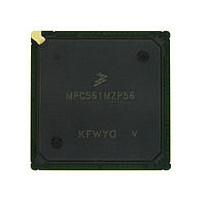
MPC561MZP56 Freescale, MPC561MZP56 Datasheet - Page 300

MPC561MZP56
Manufacturer Part Number
MPC561MZP56
Description
Manufacturer
Freescale
Datasheet
1.MPC561MZP56.pdf
(1420 pages)
Specifications of MPC561MZP56
Cpu Family
MPC56x
Device Core
PowerPC
Device Core Size
32b
Frequency (max)
56MHz
Interface Type
QSPI/SCI/SPI/UART
Total Internal Ram Size
32KB
# I/os (max)
56
Number Of Timers - General Purpose
22
Operating Supply Voltage (typ)
2.6/5V
Operating Supply Voltage (max)
2.7/5.25V
Operating Supply Voltage (min)
2.5/4.75V
On-chip Adc
2(32-chx10-bit)
Instruction Set Architecture
RISC
Operating Temp Range
-40C to 125C
Operating Temperature Classification
Automotive
Mounting
Surface Mount
Pin Count
388
Package Type
BGA
Program Memory Type
ROMLess
Program Memory Size
Not Required
Lead Free Status / RoHS Status
Not Compliant
Available stocks
Company
Part Number
Manufacturer
Quantity
Price
Company:
Part Number:
MPC561MZP56
Manufacturer:
Freescale Semiconductor
Quantity:
10 000
Company:
Part Number:
MPC561MZP56R2
Manufacturer:
Freescale Semiconductor
Quantity:
10 000
- Current page: 300 of 1420
- Download datasheet (11Mb)
Reset
7-12
20
13:14
17:18
Bits
9:10
15
4:5
6:8
11
12
16
19
21
22
23
2
,
1
3
DBGC[0:1] Debug Pins Configuration — See
COMP
COMP
ATWC
PRPM
Name
EBDF
ETRE
FLEN
EXC_
BPS
EN_
SC
—
—
—
—
4
4
Boot Port Size — This field defines the port size of the boot device on reset (BR0[PS]). If a write
to the OR0 register occurs after reset this field definition is ignored. See
Table 10-8
00 32-bit port (default)
01 8-bit port
10 16-bit port
11 Reserved
Reserved. These bits must not be high in the reset configuration word.
(SIUMCR),” for this field definition. The default value is that these pins function as: VFLS[0:1], BI,
BR, BG and BB. See
Reserved.
Address Type Write Enable Configuration — The default value is that these pins function as WE
pins. See
0 WE[0:3]/BE[0:3]/AT[0:3] functions as WE[0:3]/BE[0:3]
1 WE[0:3]/BE[0:3]/AT[0:3] functions as AT[0:3]
External Bus Division Factor — This field defines the initial value of the external bus frequency.
The default value is that CLKOUT frequency is equal to that of the internal clock (no division).
See
Reserved. This bit must be 0 in the reset configuration word.
Peripheral Mode Enable — This bit determines if the chip is in peripheral mode. A detailed
description is in
Single Chip Select — This field defines the mode of theMPC562/MPC564. See
00 Extended chip, 32 bits data
01 Extended chip, 16 bits data
10 Single chip and show cycles (address)
11 Single chip
Exception Table Relocation Enable — This field defines whether the Exception Table Relocation
feature in the BBC is enabled or disabled; The default state for this field is disabled. For more
details, see
Flash Enable — This field determines whether the on-chip Flash memory is enabled or disabled
out of reset. The default state is disabled, which means that by default, the boot is from external
memory. Refer to
0 Flash disabled — boot is from external memory
1 Flash enabled
Enable Compression — This bit enables the operation of the MPC562/MPC564 with compressed
code. The default state is disabled. See
“MPC562/MPC564 Compression Features."
Exception Compression — This bit determines the operation of the MPC562/MPC564 with
exceptions. If this bit is set, then the MPC562/MPC564 assumes that ALL the exception routines
are in compressed code. The default indicates the exceptions are all non-compressed. See
Table 4-4
Reserved. This bit must not be high in the reset configuration word.
Table
and <XrefBlue>Appendix A, “MPC562/MPC564 Compression Features."
Table 7-5. RCW Bit Descriptions (continued)
Table
8-9.
for more information.
Table
MPC561/MPC563 Reference Manual, Rev. 1.2
6-7.
Table 6-13
Table 6-12
4-4.
Table
The default value is no peripheral mode enabled.
6-8.
for more details.
Section 6.2.2.1.1, “SIU Module Configuration Register
Table 4-4
Description
and <XrefBlue>Appendix A,
Table 10-5
Freescale Semiconductor
Table
and
6-10.
Related parts for MPC561MZP56
Image
Part Number
Description
Manufacturer
Datasheet
Request
R

Part Number:
Description:
MPC5 1K0 5%
Manufacturer:
TE Connectivity
Datasheet:

Part Number:
Description:
MPC5 500R 5%
Manufacturer:
TE Connectivity
Datasheet:

Part Number:
Description:
MPC5 5K0 5%
Manufacturer:
Tyco Electronics
Datasheet:

Part Number:
Description:
MPC5 5R0 5%
Manufacturer:
Tyco Electronics
Datasheet:

Part Number:
Description:
MPC5 50K 5%
Manufacturer:
Tyco Electronics
Datasheet:

Part Number:
Description:
MPC5 1R0 5%
Manufacturer:
Tyco Electronics
Datasheet:

Part Number:
Description:
TOWER ELEVATOR BOARDS HARDWARE
Manufacturer:
Freescale Semiconductor
Datasheet:

Part Number:
Description:
TOWER SERIAL I/O HARDWARE
Manufacturer:
Freescale Semiconductor
Datasheet:

Part Number:
Description:
LCD MODULE FOR TWR SYSTEM
Manufacturer:
Freescale Semiconductor
Datasheet:

Part Number:
Description:
DAUGHTER LCD WVGA I.MX51
Manufacturer:
Freescale Semiconductor
Datasheet:

Part Number:
Description:
TOWER SYSTEM BOARD MPC5125
Manufacturer:
Freescale Semiconductor
Datasheet:


