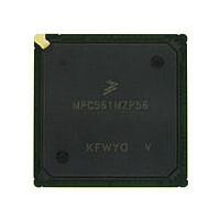
MPC561MZP56 Freescale, MPC561MZP56 Datasheet - Page 127

MPC561MZP56
Manufacturer Part Number
MPC561MZP56
Description
Manufacturer
Freescale
Datasheet
1.MPC561MZP56.pdf
(1420 pages)
Specifications of MPC561MZP56
Cpu Family
MPC56x
Device Core
PowerPC
Device Core Size
32b
Frequency (max)
56MHz
Interface Type
QSPI/SCI/SPI/UART
Total Internal Ram Size
32KB
# I/os (max)
56
Number Of Timers - General Purpose
22
Operating Supply Voltage (typ)
2.6/5V
Operating Supply Voltage (max)
2.7/5.25V
Operating Supply Voltage (min)
2.5/4.75V
On-chip Adc
2(32-chx10-bit)
Instruction Set Architecture
RISC
Operating Temp Range
-40C to 125C
Operating Temperature Classification
Automotive
Mounting
Surface Mount
Pin Count
388
Package Type
BGA
Program Memory Type
ROMLess
Program Memory Size
Not Required
Lead Free Status / RoHS Status
Not Compliant
Available stocks
Company
Part Number
Manufacturer
Quantity
Price
Company:
Part Number:
MPC561MZP56
Manufacturer:
Freescale Semiconductor
Quantity:
10 000
Company:
Part Number:
MPC561MZP56R2
Manufacturer:
Freescale Semiconductor
Quantity:
10 000
- Current page: 127 of 1420
- Download datasheet (11Mb)
2.5.1
The MPC561/MPC563 has five JTAG signals. The test data input (TDI) and test data output (TDO) scan
ports are used to scan instructions as well as data into the various scan registers for JTAG operations. The
scan operation is controlled by the test access port (TAP) controller, which in turn is controlled by the test
mode select (TMS) input sequence. The scan data is latched at the rising edge of the test clock (TCK).
On the MPC561/MPC563, JTAG is used for boundary scan only. There is no access to internal
MPC561/MPC563 circuitry. When JTAG mode is enabled, the READI module will be held inactive. See
Figure 2-4
JTAG is entered by the following sequence of events:
JTAG mode is exited by:
Freescale Semiconductor
•
•
•
Assert PORESET/TRST to reset the JTAG TAP controller
Hold JCOMP/RSTI high prior to PORESET/TRST negation and keep high as long as JTAG mode
is required
(The READI module will be held inactive since only one of the multiplexed functions JCOMP and
RSTI can be asserted at the negation of PORESET/TRST).
Drive JCOMP/RSTI low.
for JTAG mode selection.
JTAG Mode Selection
JCOMP
Signal
DSCK
DSDI
MDI0
EVTI
PORESET/TRST and analog signals ANx, EXTAL, XTAL, and
TDI/TDO/TMS/TCK are not in the JTAG scan path.
Table 2-13. MPC561/MPC563 Mode Selection Options
MPC561/MPC563 Reference Manual, Rev. 1.2
State
High
High
High
High
High
Low
Low
Low
Low
Low
Nexus Configuration
JTAG Selection
BDM Mode
NOTE
8 clocks after SRESET
8 clocks after SRESET
SRESET negation
SRESET negation
When Sampled
RSTI negation
RSTI negation
EVTI negation
EVTI negation
PORESET
PORESET
READI module Disabled
READI module Enabled
Nexus or BDM allowed
JTAG Mode Selected
Asynchronous mode
BDM mode disabled
BDM mode enabled
Reduced port mode
Synchronous mode
Full Port mode
Affect
Signal Descriptions
2-29
Related parts for MPC561MZP56
Image
Part Number
Description
Manufacturer
Datasheet
Request
R

Part Number:
Description:
MPC5 1K0 5%
Manufacturer:
TE Connectivity
Datasheet:

Part Number:
Description:
MPC5 500R 5%
Manufacturer:
TE Connectivity
Datasheet:

Part Number:
Description:
MPC5 5K0 5%
Manufacturer:
Tyco Electronics
Datasheet:

Part Number:
Description:
MPC5 5R0 5%
Manufacturer:
Tyco Electronics
Datasheet:

Part Number:
Description:
MPC5 50K 5%
Manufacturer:
Tyco Electronics
Datasheet:

Part Number:
Description:
MPC5 1R0 5%
Manufacturer:
Tyco Electronics
Datasheet:

Part Number:
Description:
TOWER ELEVATOR BOARDS HARDWARE
Manufacturer:
Freescale Semiconductor
Datasheet:

Part Number:
Description:
TOWER SERIAL I/O HARDWARE
Manufacturer:
Freescale Semiconductor
Datasheet:

Part Number:
Description:
LCD MODULE FOR TWR SYSTEM
Manufacturer:
Freescale Semiconductor
Datasheet:

Part Number:
Description:
DAUGHTER LCD WVGA I.MX51
Manufacturer:
Freescale Semiconductor
Datasheet:

Part Number:
Description:
TOWER SYSTEM BOARD MPC5125
Manufacturer:
Freescale Semiconductor
Datasheet:


