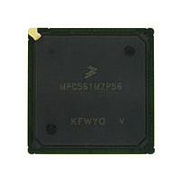
MPC561MZP56 Freescale, MPC561MZP56 Datasheet - Page 952

MPC561MZP56
Manufacturer Part Number
MPC561MZP56
Description
Manufacturer
Freescale
Datasheet
1.MPC561MZP56.pdf
(1420 pages)
Specifications of MPC561MZP56
Cpu Family
MPC56x
Device Core
PowerPC
Device Core Size
32b
Frequency (max)
56MHz
Interface Type
QSPI/SCI/SPI/UART
Total Internal Ram Size
32KB
# I/os (max)
56
Number Of Timers - General Purpose
22
Operating Supply Voltage (typ)
2.6/5V
Operating Supply Voltage (max)
2.7/5.25V
Operating Supply Voltage (min)
2.5/4.75V
On-chip Adc
2(32-chx10-bit)
Instruction Set Architecture
RISC
Operating Temp Range
-40C to 125C
Operating Temperature Classification
Automotive
Mounting
Surface Mount
Pin Count
388
Package Type
BGA
Program Memory Type
ROMLess
Program Memory Size
Not Required
Lead Free Status / RoHS Status
Not Compliant
Available stocks
Company
Part Number
Manufacturer
Quantity
Price
Company:
Part Number:
MPC561MZP56
Manufacturer:
Freescale Semiconductor
Quantity:
10 000
Company:
Part Number:
MPC561MZP56R2
Manufacturer:
Freescale Semiconductor
Quantity:
10 000
- Current page: 952 of 1420
- Download datasheet (11Mb)
Development Support
For large blocks of data this sequence may take significant time to complete. The “fast download
procedure” of the debug port may be used to reduce this time. This time reduction is achieved by
eliminating the need to transfer the instructions in the loop to the debug port. The only transactions needed
are those required to transfer the data to be placed in system memory.
illustrate the time benefit of the “fast download procedure”.
The sequence of the instructions used in the “fast download procedure” is the one illustrated in
Figure 23-12
procedure” command is issued to the debug port.
Note that, the internal general purpose register 31 is used for temporary storage data value. Before
beginning the “fast download procedure” by the “start download procedure command”, The value of the
first memory block address, – 4, must be written to the general purpose register 30.
To end a download procedure, an “end download procedure” command should be issued to the debug port,
and then, additional DATA transaction should be sent by the development tool. This data word will NOT
be placed into the system memory, but it is needed to stop the procedure gracefully.
23.5
When in debug mode disable, a software monitor debugger can make use of all of the development support
features defined in the CPU. When debug mode is disabled all events result in regular interrupt handling,
i.e. the processor resumes execution in the corresponding interrupt handler. The exception cause register
(ECR) and the debug enable register (DER) only influence the assertion and negation of the freeze signal.
23.5.1
The internal freeze signal is connected to all relevant internal modules. These modules can be programmed
to stop all operations in response to the assertion of the freeze signal. In order to enable a software monitor
debugger to broadcast the fact that the debug software is now executed, it is possible to assert and negate
the internal freeze signal also when debug mode is disabled.
23-38
Internal
Activity
Internal
Activity
External
Transaction
External
Transaction
Software Monitor Debugger Support
Freeze Indication
with RX = r31 and RY = r30. This sequence is repeated infinitely until the “end download
MFSPR
Figure 23-13. Slow Download Procedure Loop
Figure 23-14. Fast Download Procedure Loop
MPC561/MPC563 Reference Manual, Rev. 1.2
DATA
DATA
Figure 23-13
STWU
and
Freescale Semiconductor
Figure 23-14
Related parts for MPC561MZP56
Image
Part Number
Description
Manufacturer
Datasheet
Request
R

Part Number:
Description:
MPC5 1K0 5%
Manufacturer:
TE Connectivity
Datasheet:

Part Number:
Description:
MPC5 500R 5%
Manufacturer:
TE Connectivity
Datasheet:

Part Number:
Description:
MPC5 5K0 5%
Manufacturer:
Tyco Electronics
Datasheet:

Part Number:
Description:
MPC5 5R0 5%
Manufacturer:
Tyco Electronics
Datasheet:

Part Number:
Description:
MPC5 50K 5%
Manufacturer:
Tyco Electronics
Datasheet:

Part Number:
Description:
MPC5 1R0 5%
Manufacturer:
Tyco Electronics
Datasheet:

Part Number:
Description:
TOWER ELEVATOR BOARDS HARDWARE
Manufacturer:
Freescale Semiconductor
Datasheet:

Part Number:
Description:
TOWER SERIAL I/O HARDWARE
Manufacturer:
Freescale Semiconductor
Datasheet:

Part Number:
Description:
LCD MODULE FOR TWR SYSTEM
Manufacturer:
Freescale Semiconductor
Datasheet:

Part Number:
Description:
DAUGHTER LCD WVGA I.MX51
Manufacturer:
Freescale Semiconductor
Datasheet:

Part Number:
Description:
TOWER SYSTEM BOARD MPC5125
Manufacturer:
Freescale Semiconductor
Datasheet:


