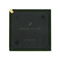
MPC561MZP56 Freescale, MPC561MZP56 Datasheet - Page 1356

MPC561MZP56
Manufacturer Part Number
MPC561MZP56
Description
Manufacturer
Freescale
Datasheet
1.MPC561MZP56.pdf
(1420 pages)
Specifications of MPC561MZP56
Cpu Family
MPC56x
Device Core
PowerPC
Device Core Size
32b
Frequency (max)
56MHz
Interface Type
QSPI/SCI/SPI/UART
Total Internal Ram Size
32KB
# I/os (max)
56
Number Of Timers - General Purpose
22
Operating Supply Voltage (typ)
2.6/5V
Operating Supply Voltage (max)
2.7/5.25V
Operating Supply Voltage (min)
2.5/4.75V
On-chip Adc
2(32-chx10-bit)
Instruction Set Architecture
RISC
Operating Temp Range
-40C to 125C
Operating Temperature Classification
Automotive
Mounting
Surface Mount
Pin Count
388
Package Type
BGA
Program Memory Type
ROMLess
Program Memory Size
Not Required
Lead Free Status / RoHS Status
Not Compliant
Available stocks
Company
Part Number
Manufacturer
Quantity
Price
Company:
Part Number:
MPC561MZP56
Manufacturer:
Freescale Semiconductor
Quantity:
10 000
Company:
Part Number:
MPC561MZP56R2
Manufacturer:
Freescale Semiconductor
Quantity:
10 000
- Current page: 1356 of 1420
- Download datasheet (11Mb)
66-MHz Electrical Characteristics
G.15 QADC64E Electrical Characteristics
Note: (V
G-50
1
2
3
4
5
6
7
Num
102a
107a
100
101
102
104
105
106
107
Conversion characteristics vary with F
The number of conversion cycles is dependent on the IST bit in the CCW register.
At V
Accuracy tested and guaranteed at V
This parameter is periodically sampled rather than 100% tested.
Absolute error includes 1/2 count (~2.5 mV) of inherent quantization error and circuit (differential, integral, and
offset) error. Specification assumes that adequate low-pass filtering is present on analog input pins — capacitive filter
with 0.01 µF to 0.1 µF capacitor between analog input and analog ground, typical source isolation
impedance of 10 KΩ.
Input signals with large slew rates or high frequency noise components cannot be converted accurately. These signals
may affect the conversion accuracy of other channels.
97
98
99
DD
RH
= 2.6 V ± 0.1 V, V
QADC Clock (QCLK) Frequency
Conversion Cycles
Legacy mode: QADCMCR[FLIP] = 0
Enhanced mode: QADCMCR[FLIP] = 1
Conversion Time
F
Legacy mode: QADCMCR[FLIP] = 0
Min = CCW[IST] =0b00, CCW[BYP] = 0
Max = CCW[IST] =0b11, CCW[BYP] = 1
Enhanced mode: QADCMCR[FLIP] = 1
Min = CCW[IST] =0b0
Max = CCW[IST] =0b1
Stop Mode Recovery Time
Resolution
Absolute (total unadjusted) error
F
Absolute (total unadjusted) error
F
DC Disruptive Input Injection Current
Current Coupling Ratio
Incremental error due to injection current
All channels have same 10KΩ < Rs <100kΩ
Channel under test has Rs=10KΩ, I
Source impedance at input
Incremental capacitance during Sampling
– V
QCLK
QCLK
QCLK
PQA
PQB
RL
= 2.0 MHz
= 2.0MHz
= 2.0MHz
= 5.12 V, one count = 5 mV.
3
DDH
3
3
1
, 2 clock input sample time
, 2 clock input sample time
2
Table G-16. QADC64E Conversion Characteristics
= 5.0 V ± 0.25 V, T
Parameter
20
MPC561/MPC563 Reference Manual, Rev. 1.2
21
RH
QCLK
1
4, 5, 6, 7
8, 9, 10, 11
– V
INJ
12, 13, 14, 15, 16
rate. Reduced conversion accuracy occurs at max F
RL
=+3mA
A
= 5.0 V ± 0.25 V
= T
22
L
to T
H
)
Symbol
C
T
F
AE
I
I
INJ
INJ
E
CONV
T
QCLK
SAMP
CC
CC
AE
R
—
K
SR
INJ
ALT
S
17
18
-3
Min
-7.8
0.5
6.0
7.0
12
14
—
—
—
—
—
-2
-1
5
19
8x10
8x10
Max
+1.0
+1.0
100
3.0
3.5
28
20
14
10
10
—
2
3
1
5
Freescale Semiconductor
-5
-5
QCLK
rate.
QCLK cycles
QCLK cycles
Counts
Counts
Counts
Units
MHz
mΑ
mV
mV
mA
KΩ
pF
µs
µs
µs
µs
µs
Related parts for MPC561MZP56
Image
Part Number
Description
Manufacturer
Datasheet
Request
R

Part Number:
Description:
MPC5 1K0 5%
Manufacturer:
TE Connectivity
Datasheet:

Part Number:
Description:
MPC5 500R 5%
Manufacturer:
TE Connectivity
Datasheet:

Part Number:
Description:
MPC5 5K0 5%
Manufacturer:
Tyco Electronics
Datasheet:

Part Number:
Description:
MPC5 5R0 5%
Manufacturer:
Tyco Electronics
Datasheet:

Part Number:
Description:
MPC5 50K 5%
Manufacturer:
Tyco Electronics
Datasheet:

Part Number:
Description:
MPC5 1R0 5%
Manufacturer:
Tyco Electronics
Datasheet:

Part Number:
Description:
TOWER ELEVATOR BOARDS HARDWARE
Manufacturer:
Freescale Semiconductor
Datasheet:

Part Number:
Description:
TOWER SERIAL I/O HARDWARE
Manufacturer:
Freescale Semiconductor
Datasheet:

Part Number:
Description:
LCD MODULE FOR TWR SYSTEM
Manufacturer:
Freescale Semiconductor
Datasheet:

Part Number:
Description:
DAUGHTER LCD WVGA I.MX51
Manufacturer:
Freescale Semiconductor
Datasheet:

Part Number:
Description:
TOWER SYSTEM BOARD MPC5125
Manufacturer:
Freescale Semiconductor
Datasheet:


