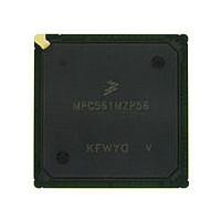
MPC561MZP56 Freescale, MPC561MZP56 Datasheet - Page 771

MPC561MZP56
Manufacturer Part Number
MPC561MZP56
Description
Manufacturer
Freescale
Datasheet
1.MPC561MZP56.pdf
(1420 pages)
Specifications of MPC561MZP56
Cpu Family
MPC56x
Device Core
PowerPC
Device Core Size
32b
Frequency (max)
56MHz
Interface Type
QSPI/SCI/SPI/UART
Total Internal Ram Size
32KB
# I/os (max)
56
Number Of Timers - General Purpose
22
Operating Supply Voltage (typ)
2.6/5V
Operating Supply Voltage (max)
2.7/5.25V
Operating Supply Voltage (min)
2.5/4.75V
On-chip Adc
2(32-chx10-bit)
Instruction Set Architecture
RISC
Operating Temp Range
-40C to 125C
Operating Temperature Classification
Automotive
Mounting
Surface Mount
Pin Count
388
Package Type
BGA
Program Memory Type
ROMLess
Program Memory Size
Not Required
Lead Free Status / RoHS Status
Not Compliant
Available stocks
Company
Part Number
Manufacturer
Quantity
Price
Company:
Part Number:
MPC561MZP56
Manufacturer:
Freescale Semiconductor
Quantity:
10 000
Company:
Part Number:
MPC561MZP56R2
Manufacturer:
Freescale Semiconductor
Quantity:
10 000
- Current page: 771 of 1420
- Download datasheet (11Mb)
In the OPWM mode, the WOR bit selects whether the output is totem pole driven or open-drain.
17.9.4
17.9.5
When the reset signal is asserted, the MDASM registers are reset according to the values specified in
Section 17.9.6, “MDASM
17.9.6
The privilege level to access the MDASM registers depends on the MIOS14MCR[SUPV]. The privilege
level is unrestricted after reset and can be changed to supervisor by software.
17.9.6.1
The MDASM register map comprises four 16-bit register locations. As shown in below, the register block
contains four MDASM registers. Note that the MDASMSCRD is the duplication of the MDASMSCR.
This is done to allow 32-bit aligned accesses.
All unused bits return zero when read by the software. All register addresses in this section are specified
as offsets from the base address of the MDASM.
Freescale Semiconductor
•
•
•
The MDASM is connected to all the signals in the read/write and control bus, to allow data transfer
from and to the MDASM registers, and to control the MDASM in the different possible situations.
The MDASM is connected to four 16-bit counter buses available to that submodule instance, so
that the MDASM can select by software which one to use.
The MDASM uses the request bus to transmit the FLAG line to the interrupt request submodule
(MIRSM).
Modular I/O Bus (MIOB) Interface
Effect of RESET on MDASM
MDASM Registers
MDASM Registers Organization
The user should not write directly to the address of the MDASMSCRD. This
register’s address may be reserved for future use and should not be accessed
by the software to ensure future software compatibility.
0x30 6058
0x30 605A
Address
Registers.”
MDASM11 Data A Register (MDASMAR)
See
descriptions.
MDASM11 Data B Register (MDASMBR)
See
descriptions.
MPC561/MPC563 Reference Manual, Rev. 1.2
Section 17.9.6.2, “MDASM Data A (MDASMAR)
Section 17.9.6.3, “MDASM Data B (MDASMBR)
Table 17-18. MDASM Address Map
WARNING
MDASM11
Register
Modular Input/Output Subsystem (MIOS14)
Register” for bit
Register” for bit
17-39
Related parts for MPC561MZP56
Image
Part Number
Description
Manufacturer
Datasheet
Request
R

Part Number:
Description:
MPC5 1K0 5%
Manufacturer:
TE Connectivity
Datasheet:

Part Number:
Description:
MPC5 500R 5%
Manufacturer:
TE Connectivity
Datasheet:

Part Number:
Description:
MPC5 5K0 5%
Manufacturer:
Tyco Electronics
Datasheet:

Part Number:
Description:
MPC5 5R0 5%
Manufacturer:
Tyco Electronics
Datasheet:

Part Number:
Description:
MPC5 50K 5%
Manufacturer:
Tyco Electronics
Datasheet:

Part Number:
Description:
MPC5 1R0 5%
Manufacturer:
Tyco Electronics
Datasheet:

Part Number:
Description:
TOWER ELEVATOR BOARDS HARDWARE
Manufacturer:
Freescale Semiconductor
Datasheet:

Part Number:
Description:
TOWER SERIAL I/O HARDWARE
Manufacturer:
Freescale Semiconductor
Datasheet:

Part Number:
Description:
LCD MODULE FOR TWR SYSTEM
Manufacturer:
Freescale Semiconductor
Datasheet:

Part Number:
Description:
DAUGHTER LCD WVGA I.MX51
Manufacturer:
Freescale Semiconductor
Datasheet:

Part Number:
Description:
TOWER SYSTEM BOARD MPC5125
Manufacturer:
Freescale Semiconductor
Datasheet:


