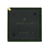
MPC561MZP56 Freescale, MPC561MZP56 Datasheet - Page 832

MPC561MZP56
Manufacturer Part Number
MPC561MZP56
Description
Manufacturer
Freescale
Datasheet
1.MPC561MZP56.pdf
(1420 pages)
Specifications of MPC561MZP56
Cpu Family
MPC56x
Device Core
PowerPC
Device Core Size
32b
Frequency (max)
56MHz
Interface Type
QSPI/SCI/SPI/UART
Total Internal Ram Size
32KB
# I/os (max)
56
Number Of Timers - General Purpose
22
Operating Supply Voltage (typ)
2.6/5V
Operating Supply Voltage (max)
2.7/5.25V
Operating Supply Voltage (min)
2.5/4.75V
On-chip Adc
2(32-chx10-bit)
Instruction Set Architecture
RISC
Operating Temp Range
-40C to 125C
Operating Temperature Classification
Automotive
Mounting
Surface Mount
Pin Count
388
Package Type
BGA
Program Memory Type
ROMLess
Program Memory Size
Not Required
Lead Free Status / RoHS Status
Not Compliant
Available stocks
Company
Part Number
Manufacturer
Quantity
Price
Company:
Part Number:
MPC561MZP56
Manufacturer:
Freescale Semiconductor
Quantity:
10 000
Company:
Part Number:
MPC561MZP56R2
Manufacturer:
Freescale Semiconductor
Quantity:
10 000
- Current page: 832 of 1420
- Download datasheet (11Mb)
Time Processor Unit 3
19.1
The TPU3 can be viewed as a special-purpose microcomputer that performs a programmable series of two
operations, match and capture. Each occurrence of either operation is called an event. A programmed
series of events is called a function. TPU functions replace software functions that would require CPU
interrupt service.
The microcode ROM TPU3 functions that are available in the MPC561/MPC563 are described in
Appendix D, “TPU3 ROM
19.2
The TPU3 consists of two 16-bit time bases, 16 independent timer channels, a task scheduler, a
microengine, and a host interface. In addition, a dual-ported parameter RAM (DPTRAM) is used to pass
parameters between the module and the CPU.
19.2.1
Two 16-bit counters provide reference time bases for all output-compare and input-capture events.
Prescalers for both time bases are controlled by the CPU via bit fields in the TPU3 module configuration
register (TPUMCR) and TPU module configuration register two (TPUMCR2). Timer count registers
TCR1 and TCR2 provide access to the current counter values. TCR1 and TCR2 can be read by TPU
microcode but are not directly available to the CPU. The TCR1 clock is always derived from the system
clock. The TCR2 clock can be derived from the system clock or from an external input via theT2CLK
clock pin. The duration between active edges on the T2CLK clock pin must be at least nine system clocks.
19.2.2
The TPU3 has 16 independent channels, each connected to an MCU pin. The channels have identical
hardware and are functionally equivalent in operation. Each channel consists of an event register and pin
control logic. The event register contains a 16-bit capture register, a 16-bit compare/match register, and a
16-bit greater-than-or-equal-to comparator. The direction of each pin, either output or input, is determined
by the TPU microengine. Each channel can either use the same time base for match and capture, or can
use one time base for match and the other for capture.
19.2.3
When a service request is received, the scheduler determines which TPU3 channel is serviced by the
microengine. A channel can request service for one of four reasons: for host service, for a link to another
channel, for a match event, or for a capture event. The host system assigns each active channel one of three
priorities: high, middle, or low. When multiple service requests are received simultaneously, a
priority-scheduling mechanism grants service based on channel number and assigned priority.
19-2
Overview
TPU3 Components
Time Bases
Timer Channels
Scheduler
Functions.”
MPC561/MPC563 Reference Manual, Rev. 1.2
Freescale Semiconductor
Related parts for MPC561MZP56
Image
Part Number
Description
Manufacturer
Datasheet
Request
R

Part Number:
Description:
MPC5 1K0 5%
Manufacturer:
TE Connectivity
Datasheet:

Part Number:
Description:
MPC5 500R 5%
Manufacturer:
TE Connectivity
Datasheet:

Part Number:
Description:
MPC5 5K0 5%
Manufacturer:
Tyco Electronics
Datasheet:

Part Number:
Description:
MPC5 5R0 5%
Manufacturer:
Tyco Electronics
Datasheet:

Part Number:
Description:
MPC5 50K 5%
Manufacturer:
Tyco Electronics
Datasheet:

Part Number:
Description:
MPC5 1R0 5%
Manufacturer:
Tyco Electronics
Datasheet:

Part Number:
Description:
TOWER ELEVATOR BOARDS HARDWARE
Manufacturer:
Freescale Semiconductor
Datasheet:

Part Number:
Description:
TOWER SERIAL I/O HARDWARE
Manufacturer:
Freescale Semiconductor
Datasheet:

Part Number:
Description:
LCD MODULE FOR TWR SYSTEM
Manufacturer:
Freescale Semiconductor
Datasheet:

Part Number:
Description:
DAUGHTER LCD WVGA I.MX51
Manufacturer:
Freescale Semiconductor
Datasheet:

Part Number:
Description:
TOWER SYSTEM BOARD MPC5125
Manufacturer:
Freescale Semiconductor
Datasheet:


