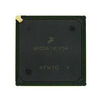
MPC561MZP56 Freescale, MPC561MZP56 Datasheet - Page 862

MPC561MZP56
Manufacturer Part Number
MPC561MZP56
Description
Manufacturer
Freescale
Datasheet
1.MPC561MZP56.pdf
(1420 pages)
Specifications of MPC561MZP56
Cpu Family
MPC56x
Device Core
PowerPC
Device Core Size
32b
Frequency (max)
56MHz
Interface Type
QSPI/SCI/SPI/UART
Total Internal Ram Size
32KB
# I/os (max)
56
Number Of Timers - General Purpose
22
Operating Supply Voltage (typ)
2.6/5V
Operating Supply Voltage (max)
2.7/5.25V
Operating Supply Voltage (min)
2.5/4.75V
On-chip Adc
2(32-chx10-bit)
Instruction Set Architecture
RISC
Operating Temp Range
-40C to 125C
Operating Temperature Classification
Automotive
Mounting
Surface Mount
Pin Count
388
Package Type
BGA
Program Memory Type
ROMLess
Program Memory Size
Not Required
Lead Free Status / RoHS Status
Not Compliant
Available stocks
Company
Part Number
Manufacturer
Quantity
Price
Company:
Part Number:
MPC561MZP56
Manufacturer:
Freescale Semiconductor
Quantity:
10 000
Company:
Part Number:
MPC561MZP56R2
Manufacturer:
Freescale Semiconductor
Quantity:
10 000
- Current page: 862 of 1420
- Download datasheet (11Mb)
Dual-Port TPU3 RAM (DPTRAM)
When the DPTRAM array is being used by one or two of the TPU3 units, all accesses via the IMB3 are
disabled. The control registers have no effect on the RAM array.
The contents of the RAM are validated using a multiple input signature calculator (MISC). MISC reads of
the RAM are performed only when the MPC561/MPC563 is in emulation mode and the MISC is enabled
(MISEN = 1 in the DPTMCR).
Refer to
Section 19.3.6, “Emulation
Support” for more information in TPU3 and DPTRAM operation in
emulation mode.
20.5
Multiple Input Signature Calculator (MISC)
The integrity of the DPTRAM data is ensured through the use of a MISC. The DPTRAM data is read in
reverse address order and a unique 32-bit signature is generated based on the output of these reads. MISC
reads are performed when one of the TPU3 modules does not request back-to-back accesses to the
DPTRAM provided that the MISEN bit in the DPTMCR is set.
The MISC generates the DPTRAM signature based on the following polynomial:
31
2
22
G x ( )
=
1
+ +
x
x
+
x
+
x
Eqn. 20-1
After the entire DPTRAM has been read and a signature has been calculated, the MISC sets the MISF bit
in the DPTMCR. The host should poll this bit and enter a handling routine when the bit is found to be set.
The signature should then be read from the MISRH and MISRL registers and the host determines if it
matches the predetermined signature.
The MISRH and MISRL registers are updated each time the MISC completes reading the entire DPTRAM
regardless of whether or not the previous signature has been read or not. This ensures that the host reads
the most recently generated signature.
The MISC can be disabled by clearing the MISEN bit in the DPTMCR.
NOTE
The reset state of the DPTMCR[MISEN] is disabled.
MPC561/MPC563 Reference Manual, Rev. 1.2
20-8
Freescale Semiconductor
Related parts for MPC561MZP56
Image
Part Number
Description
Manufacturer
Datasheet
Request
R

Part Number:
Description:
MPC5 1K0 5%
Manufacturer:
TE Connectivity
Datasheet:

Part Number:
Description:
MPC5 500R 5%
Manufacturer:
TE Connectivity
Datasheet:

Part Number:
Description:
MPC5 5K0 5%
Manufacturer:
Tyco Electronics
Datasheet:

Part Number:
Description:
MPC5 5R0 5%
Manufacturer:
Tyco Electronics
Datasheet:

Part Number:
Description:
MPC5 50K 5%
Manufacturer:
Tyco Electronics
Datasheet:

Part Number:
Description:
MPC5 1R0 5%
Manufacturer:
Tyco Electronics
Datasheet:

Part Number:
Description:
TOWER ELEVATOR BOARDS HARDWARE
Manufacturer:
Freescale Semiconductor
Datasheet:

Part Number:
Description:
TOWER SERIAL I/O HARDWARE
Manufacturer:
Freescale Semiconductor
Datasheet:

Part Number:
Description:
LCD MODULE FOR TWR SYSTEM
Manufacturer:
Freescale Semiconductor
Datasheet:

Part Number:
Description:
DAUGHTER LCD WVGA I.MX51
Manufacturer:
Freescale Semiconductor
Datasheet:

Part Number:
Description:
TOWER SYSTEM BOARD MPC5125
Manufacturer:
Freescale Semiconductor
Datasheet:


