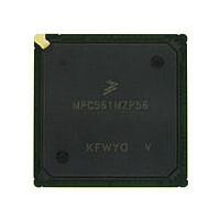
MPC561MZP56 Freescale, MPC561MZP56 Datasheet - Page 354

MPC561MZP56
Manufacturer Part Number
MPC561MZP56
Description
Manufacturer
Freescale
Datasheet
1.MPC561MZP56.pdf
(1420 pages)
Specifications of MPC561MZP56
Cpu Family
MPC56x
Device Core
PowerPC
Device Core Size
32b
Frequency (max)
56MHz
Interface Type
QSPI/SCI/SPI/UART
Total Internal Ram Size
32KB
# I/os (max)
56
Number Of Timers - General Purpose
22
Operating Supply Voltage (typ)
2.6/5V
Operating Supply Voltage (max)
2.7/5.25V
Operating Supply Voltage (min)
2.5/4.75V
On-chip Adc
2(32-chx10-bit)
Instruction Set Architecture
RISC
Operating Temp Range
-40C to 125C
Operating Temperature Classification
Automotive
Mounting
Surface Mount
Pin Count
388
Package Type
BGA
Program Memory Type
ROMLess
Program Memory Size
Not Required
Lead Free Status / RoHS Status
Not Compliant
Available stocks
Company
Part Number
Manufacturer
Quantity
Price
Company:
Part Number:
MPC561MZP56
Manufacturer:
Freescale Semiconductor
Quantity:
10 000
Company:
Part Number:
MPC561MZP56R2
Manufacturer:
Freescale Semiconductor
Quantity:
10 000
- Current page: 354 of 1420
- Download datasheet (11Mb)
External Bus Interface
9.5.2.3
The general case of single beat transfers assumes that the external memory has a 32-bit port size. The
MPC561/MPC563 provides an effective mechanism for interfacing with 16-bit and 8-bit port size
memories, allowing transfers to these devices when they are controlled by the internal memory controller.
In this case, the MPC561/MPC563 attempts to initiate a transfer as in the normal case. If the bus interface
receives a small port size (16 or 8 bits) indication before the transfer acknowledge to the first beat (through
the internal memory controller), the MCU initiates successive transactions until the completion of the data
transfer. Note that all the transactions initiated to complete the data transfer are considered to be part of an
atomic transaction, so the MCU does not allow other unrelated master accesses or bus arbitration to
intervene between the transfers. If any of the transactions except the first is re-tried during an access to a
small port, then a machine-check exception is generated to the RCPU.
9-14
CLKOUT
BR
BG
BB
ADDR[8:31]
RD/WR
TSIZ[0:1]
BURST, BDIP
TS
Data
TA
Single Beat Flow with Small Port Size
Figure 9-9. Single Beat Basic Write Cycle Timing – One Wait State
O
O
MPC561/MPC563 Reference Manual, Rev. 1.2
Receive bus grant and bus busy negated
O
O
Assert BB, drive address and assert TS
Wait state
O
Data is sampled
Freescale Semiconductor
Related parts for MPC561MZP56
Image
Part Number
Description
Manufacturer
Datasheet
Request
R

Part Number:
Description:
MPC5 1K0 5%
Manufacturer:
TE Connectivity
Datasheet:

Part Number:
Description:
MPC5 500R 5%
Manufacturer:
TE Connectivity
Datasheet:

Part Number:
Description:
MPC5 5K0 5%
Manufacturer:
Tyco Electronics
Datasheet:

Part Number:
Description:
MPC5 5R0 5%
Manufacturer:
Tyco Electronics
Datasheet:

Part Number:
Description:
MPC5 50K 5%
Manufacturer:
Tyco Electronics
Datasheet:

Part Number:
Description:
MPC5 1R0 5%
Manufacturer:
Tyco Electronics
Datasheet:

Part Number:
Description:
TOWER ELEVATOR BOARDS HARDWARE
Manufacturer:
Freescale Semiconductor
Datasheet:

Part Number:
Description:
TOWER SERIAL I/O HARDWARE
Manufacturer:
Freescale Semiconductor
Datasheet:

Part Number:
Description:
LCD MODULE FOR TWR SYSTEM
Manufacturer:
Freescale Semiconductor
Datasheet:

Part Number:
Description:
DAUGHTER LCD WVGA I.MX51
Manufacturer:
Freescale Semiconductor
Datasheet:

Part Number:
Description:
TOWER SYSTEM BOARD MPC5125
Manufacturer:
Freescale Semiconductor
Datasheet:


