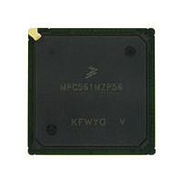
MPC561MZP56 Freescale, MPC561MZP56 Datasheet - Page 1103

MPC561MZP56
Manufacturer Part Number
MPC561MZP56
Description
Manufacturer
Freescale
Datasheet
1.MPC561MZP56.pdf
(1420 pages)
Specifications of MPC561MZP56
Cpu Family
MPC56x
Device Core
PowerPC
Device Core Size
32b
Frequency (max)
56MHz
Interface Type
QSPI/SCI/SPI/UART
Total Internal Ram Size
32KB
# I/os (max)
56
Number Of Timers - General Purpose
22
Operating Supply Voltage (typ)
2.6/5V
Operating Supply Voltage (max)
2.7/5.25V
Operating Supply Voltage (min)
2.5/4.75V
On-chip Adc
2(32-chx10-bit)
Instruction Set Architecture
RISC
Operating Temp Range
-40C to 125C
Operating Temperature Classification
Automotive
Mounting
Surface Mount
Pin Count
388
Package Type
BGA
Program Memory Type
ROMLess
Program Memory Size
Not Required
Lead Free Status / RoHS Status
Not Compliant
Available stocks
Company
Part Number
Manufacturer
Quantity
Price
Company:
Part Number:
MPC561MZP56
Manufacturer:
Freescale Semiconductor
Quantity:
10 000
Company:
Part Number:
MPC561MZP56R2
Manufacturer:
Freescale Semiconductor
Quantity:
10 000
- Current page: 1103 of 1420
- Download datasheet (11Mb)
A.3.1.1
Refer to
A.3.1.2
In this mode, the MPC562/MPC564’s RCPU sends the two-bit aligned change of flow (COF) address to
the BBC. The BIU transfers the word portion of the address to the U-bus. The BBC continues to pre-fetch
the data from the consequent memory addresses regardless of whether the RCPU requests them in order
to supply data to the ICDU.
In the MPC562/MPC564, the data coming from the instruction memory is not provided directly to the
RCPU, but loaded into the ICDU for decompression. Decompressed instruction code together with “next
instruction address” are provided to the RCPU whenever it requires another instruction fetch.
All addresses issued by the BIU to the U-bus are transferred in parallel to the IMPU. The IMPU compares
the address of the access to its region programming. If any protection violation is detected by the IMPU,
the current U-bus access is aborted by the BIU and an instruction storage protection error exception is
signaled to the RCPU.
Show cycle and program trace access attributes accompanying the COF RCPU access only are forwarded
by the BIU along with the U-bus access. Additional information about the IP of the compressed instruction
address is provided on the U-bus data bus. Refer below to
Decompression On
In this mode the MPC562/MPC564’s ICDU DECRAM is used as a decompressor vocabulary storage and
may not be used as a general purpose RAM.
A.3.1.2.1
In the MPC562/MPC564’s decompression on mode, the instruction address consists of an instruction base
address and four bits of the instruction bit pointer. In order to provide the capability to show full instruction
address, including instruction bit pointer on the external bus, show cycle information is presented not only
on the address bus, but also on some bits of the data bus:
Instruction show cycle bus transactions have the following characteristics (see
Freescale Semiconductor
•
•
•
•
•
•
ADDR[0:29] – show the value of the base address of compressed instruction (word pointer into the
memory)
DATA[0] – shows in which mode the MPC562/MPC564 is operating
— 0 = decompression off mode
— 1 = decompression on mode
DATA[1:4] – represent an instruction bit pointer within the word.
One clock cycle
Address phase only; in decompression on mode part of the compressed address is driven on data
lines together with address lines. The external bus interface adds one clock delay between a read
cycle and such show cycle.
STS assertion only (no TA assertion)
Section 4.2.1.1, “Decompression Off
Decompression Off Mode
Decompression On Mode
Show Cycles in Decompression On Mode
Mode,” for more details.
MPC561/MPC563 Reference Manual, Rev. 1.2
Mode” for an explanation of decompression off.
Section A.3.1.2.1, “Show Cycles in
MPC562/MPC564 Compression Features
Figure
9-41):
A-15
Related parts for MPC561MZP56
Image
Part Number
Description
Manufacturer
Datasheet
Request
R

Part Number:
Description:
MPC5 1K0 5%
Manufacturer:
TE Connectivity
Datasheet:

Part Number:
Description:
MPC5 500R 5%
Manufacturer:
TE Connectivity
Datasheet:

Part Number:
Description:
MPC5 5K0 5%
Manufacturer:
Tyco Electronics
Datasheet:

Part Number:
Description:
MPC5 5R0 5%
Manufacturer:
Tyco Electronics
Datasheet:

Part Number:
Description:
MPC5 50K 5%
Manufacturer:
Tyco Electronics
Datasheet:

Part Number:
Description:
MPC5 1R0 5%
Manufacturer:
Tyco Electronics
Datasheet:

Part Number:
Description:
TOWER ELEVATOR BOARDS HARDWARE
Manufacturer:
Freescale Semiconductor
Datasheet:

Part Number:
Description:
TOWER SERIAL I/O HARDWARE
Manufacturer:
Freescale Semiconductor
Datasheet:

Part Number:
Description:
LCD MODULE FOR TWR SYSTEM
Manufacturer:
Freescale Semiconductor
Datasheet:

Part Number:
Description:
DAUGHTER LCD WVGA I.MX51
Manufacturer:
Freescale Semiconductor
Datasheet:

Part Number:
Description:
TOWER SYSTEM BOARD MPC5125
Manufacturer:
Freescale Semiconductor
Datasheet:


