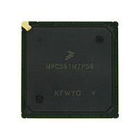
MPC561MZP56 Freescale, MPC561MZP56 Datasheet - Page 891

MPC561MZP56
Manufacturer Part Number
MPC561MZP56
Description
Manufacturer
Freescale
Datasheet
1.MPC561MZP56.pdf
(1420 pages)
Specifications of MPC561MZP56
Cpu Family
MPC56x
Device Core
PowerPC
Device Core Size
32b
Frequency (max)
56MHz
Interface Type
QSPI/SCI/SPI/UART
Total Internal Ram Size
32KB
# I/os (max)
56
Number Of Timers - General Purpose
22
Operating Supply Voltage (typ)
2.6/5V
Operating Supply Voltage (max)
2.7/5.25V
Operating Supply Voltage (min)
2.5/4.75V
On-chip Adc
2(32-chx10-bit)
Instruction Set Architecture
RISC
Operating Temp Range
-40C to 125C
Operating Temperature Classification
Automotive
Mounting
Surface Mount
Pin Count
388
Package Type
BGA
Program Memory Type
ROMLess
Program Memory Size
Not Required
Lead Free Status / RoHS Status
Not Compliant
Available stocks
Company
Part Number
Manufacturer
Quantity
Price
Company:
Part Number:
MPC561MZP56
Manufacturer:
Freescale Semiconductor
Quantity:
10 000
Company:
Part Number:
MPC561MZP56R2
Manufacturer:
Freescale Semiconductor
Quantity:
10 000
- Current page: 891 of 1420
- Download datasheet (11Mb)
With STOP = 1, the UC3F module enters a low power state by shutting down internal timers and bias
generators. A stop recovery time of 1 µs is required when clearing the STOP bit to exit stop operation. The
BIU should allow 1 µs following the negation of the STOP bit so that internal bias generators used by the
array may recover to normal levels prior to initiating any UC3F array accesses.
21.3.10 Disabled
The UC3F module can be disabled by clearing the FLEN bit in the IMMR register (see
“System Configuration and Protection
down. The register block and array are not accessible in this mode, and all circuits which draw any DC
power are disabled to eliminate power consumption. In addition,the module can be disabled by setting the
STOP bit in the UC3FMCR register (see
(UC3FMCR)”).
If the UC3F module is disabled while programming or erasing, the HSUS bit in the UC3FCTL register is
asserted (HSUS = 1) to suspend the current program or erase operation. When the UC3F module is
re-enabled, the suspended program or erase operation may be resumed by writing the HSUS bit to a 0.
When disabled, the power used by the UC3F is reduced to leakage levels; otherwise, the UC3F module is
enabled for accesses. For example, recovering from a stop operation (STOP = 1), there is a recovery time
of 1 µs for internal biases to reach to operating levels.
21.3.11 Censored Accesses and Non-Censored Accesses
The UC3F EEPROM has a censorship mechanism which provides for several censorship states. The
censorship mechanism is used to increase restrictions in accessing Flash data. Four bits in UC3FMCR are
used to configure the UC3F censorship state. These bits are:
The device has two relevant modes used by the UC3F EEPROM to select the type of censorship. The first
mode, which is uncensored mode, provides no censorship. In uncensored mode the ACCESS and
CENSOR[0:1] bits are irrelevant. The second mode, censored mode, enables the UC3F EEPROM to
exercise censorship based on the state of ACCESS, FIC, and CENSOR[0:1]. The device will enter
censored mode only if one of following events occurs:
Freescale Semiconductor
•
•
•
•
ACCESS—Enables a UC3F EEPROM to bypass the censorship.
FIC—Overrides CENSOR[0:1] to force information censorship.
CENSOR[0:1]—Determine the censorship state of the UC3F.
booting from external memory
The UC3F cannot be stopped while the array is being programmed or erased
since the STOP bit is write locked by SES = 1.
While there should be no harmful side effects resulting from disabling the
UC3F module while in program or erase operation, it is not recommended
that program or erase operation be suspended in this manner.
MPC561/MPC563 Reference Manual, Rev. 1.2
Registers”). While disabled, the UC3F module is completely shut
Section 21.2.1.2, “UC3F EEPROM Configuration Register
NOTE
NOTE
CDR3 Flash (UC3F) EEPROM
Section 6.2.2,
21-29
Related parts for MPC561MZP56
Image
Part Number
Description
Manufacturer
Datasheet
Request
R

Part Number:
Description:
MPC5 1K0 5%
Manufacturer:
TE Connectivity
Datasheet:

Part Number:
Description:
MPC5 500R 5%
Manufacturer:
TE Connectivity
Datasheet:

Part Number:
Description:
MPC5 5K0 5%
Manufacturer:
Tyco Electronics
Datasheet:

Part Number:
Description:
MPC5 5R0 5%
Manufacturer:
Tyco Electronics
Datasheet:

Part Number:
Description:
MPC5 50K 5%
Manufacturer:
Tyco Electronics
Datasheet:

Part Number:
Description:
MPC5 1R0 5%
Manufacturer:
Tyco Electronics
Datasheet:

Part Number:
Description:
TOWER ELEVATOR BOARDS HARDWARE
Manufacturer:
Freescale Semiconductor
Datasheet:

Part Number:
Description:
TOWER SERIAL I/O HARDWARE
Manufacturer:
Freescale Semiconductor
Datasheet:

Part Number:
Description:
LCD MODULE FOR TWR SYSTEM
Manufacturer:
Freescale Semiconductor
Datasheet:

Part Number:
Description:
DAUGHTER LCD WVGA I.MX51
Manufacturer:
Freescale Semiconductor
Datasheet:

Part Number:
Description:
TOWER SYSTEM BOARD MPC5125
Manufacturer:
Freescale Semiconductor
Datasheet:


