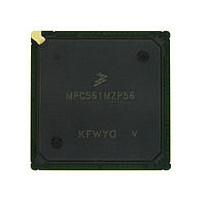
MPC561MZP56 Freescale, MPC561MZP56 Datasheet - Page 571

MPC561MZP56
Manufacturer Part Number
MPC561MZP56
Description
Manufacturer
Freescale
Datasheet
1.MPC561MZP56.pdf
(1420 pages)
Specifications of MPC561MZP56
Cpu Family
MPC56x
Device Core
PowerPC
Device Core Size
32b
Frequency (max)
56MHz
Interface Type
QSPI/SCI/SPI/UART
Total Internal Ram Size
32KB
# I/os (max)
56
Number Of Timers - General Purpose
22
Operating Supply Voltage (typ)
2.6/5V
Operating Supply Voltage (max)
2.7/5.25V
Operating Supply Voltage (min)
2.5/4.75V
On-chip Adc
2(32-chx10-bit)
Instruction Set Architecture
RISC
Operating Temp Range
-40C to 125C
Operating Temperature Classification
Automotive
Mounting
Surface Mount
Pin Count
388
Package Type
BGA
Program Memory Type
ROMLess
Program Memory Size
Not Required
Lead Free Status / RoHS Status
Not Compliant
Available stocks
Company
Part Number
Manufacturer
Quantity
Price
Company:
Part Number:
MPC561MZP56
Manufacturer:
Freescale Semiconductor
Quantity:
10 000
Company:
Part Number:
MPC561MZP56R2
Manufacturer:
Freescale Semiconductor
Quantity:
10 000
- Current page: 571 of 1420
- Download datasheet (11Mb)
initializes the QADC64E. The remaining 6-bits are unimplemented so these read as zeros, and write
operations have no effect. Each location in the CCW table corresponds to a location in the result word
table. When a conversion is completed for a CCW entry, the 10-bit result is written in the corresponding
result word entry. The QADC64E provides 64 CCW table entries.
The beginning of queue 1 is the first location in the CCW table. The first location of queue 2 is specified
by the beginning of queue 2 pointer (BQ2) in QACR2. To dedicate the entire CCW table to queue 1, queue
2 is programmed to be in the disabled mode, and BQ2 is programmed to 64 or greater. To dedicate the
entire CCW table to queue 2, queue 1 is programmed to be in the disabled mode, and BQ2 is specified as
the first location in the CCW table
Figure 14-15
To prepare the QADC64E for a scan sequence, the software writes to the CCW table to specify the desired
channel conversions. The software also establishes the criteria for initiating the queue execution by
programming the queue operating mode. The queue operating mode determines what type of trigger event
causes queue execution to begin. A “trigger event” is used to refer to any of the ways to cause the
Freescale Semiconductor
0x27E (CCW63)
0x200 (CCW0)
P = Pause Until Next Trigger
REF = Use Alternate Reference Voltage
IST = Input Sample Time
CHAN = Channel Number and End_of_Queue Code
illustrates the operation of the queue structure.
BQ2
msb
NOTE 1: These offsets must be added to the module base address: A = 0x30 4800 or B = 0x30 4C00
6
P REF IST
1
1
10-bit Conversion
Conversion Command
Command Word
Word (CCW) Table
(CCW) Format
7
Begin Queue 1
End of Queue 1
Begin Queue 2
End of Queue 2
Figure 14-15. QADC64E Conversion Queue Operation
8
MPC561/MPC563 Reference Manual, Rev. 1.2
9
CHAN
15
lsb
Analog to Digital
Channel Select,
Sample, Hold,
Conversion
A/D Converter
and
Right Justified, Unsigned Result Format
msb
0 0
0
S
Left Justified, Unsigned Result Format
0
0
Left Justified, Signed Result Format
1
0 0 0
in Three Different 16-bit Formats
Result
Result
0
Software Readable
10-bit Result is
Result Word Table
7 8
7 8
7 8
Result
QADC64E Enhanced Mode Operation
0 0
0 0
0 0 0
0
0 0
lsb
15
15
15
0
0
Result 0
Result 63
Address Offsets:
0x280-0x2FF
0x300-0x37F
0x380-0x3FF
S = Sign bit
14-29
1
1
1
Related parts for MPC561MZP56
Image
Part Number
Description
Manufacturer
Datasheet
Request
R

Part Number:
Description:
MPC5 1K0 5%
Manufacturer:
TE Connectivity
Datasheet:

Part Number:
Description:
MPC5 500R 5%
Manufacturer:
TE Connectivity
Datasheet:

Part Number:
Description:
MPC5 5K0 5%
Manufacturer:
Tyco Electronics
Datasheet:

Part Number:
Description:
MPC5 5R0 5%
Manufacturer:
Tyco Electronics
Datasheet:

Part Number:
Description:
MPC5 50K 5%
Manufacturer:
Tyco Electronics
Datasheet:

Part Number:
Description:
MPC5 1R0 5%
Manufacturer:
Tyco Electronics
Datasheet:

Part Number:
Description:
TOWER ELEVATOR BOARDS HARDWARE
Manufacturer:
Freescale Semiconductor
Datasheet:

Part Number:
Description:
TOWER SERIAL I/O HARDWARE
Manufacturer:
Freescale Semiconductor
Datasheet:

Part Number:
Description:
LCD MODULE FOR TWR SYSTEM
Manufacturer:
Freescale Semiconductor
Datasheet:

Part Number:
Description:
DAUGHTER LCD WVGA I.MX51
Manufacturer:
Freescale Semiconductor
Datasheet:

Part Number:
Description:
TOWER SYSTEM BOARD MPC5125
Manufacturer:
Freescale Semiconductor
Datasheet:


