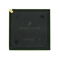
MPC561MZP56 Freescale, MPC561MZP56 Datasheet - Page 324

MPC561MZP56
Manufacturer Part Number
MPC561MZP56
Description
Manufacturer
Freescale
Datasheet
1.MPC561MZP56.pdf
(1420 pages)
Specifications of MPC561MZP56
Cpu Family
MPC56x
Device Core
PowerPC
Device Core Size
32b
Frequency (max)
56MHz
Interface Type
QSPI/SCI/SPI/UART
Total Internal Ram Size
32KB
# I/os (max)
56
Number Of Timers - General Purpose
22
Operating Supply Voltage (typ)
2.6/5V
Operating Supply Voltage (max)
2.7/5.25V
Operating Supply Voltage (min)
2.5/4.75V
On-chip Adc
2(32-chx10-bit)
Instruction Set Architecture
RISC
Operating Temp Range
-40C to 125C
Operating Temperature Classification
Automotive
Mounting
Surface Mount
Pin Count
388
Package Type
BGA
Program Memory Type
ROMLess
Program Memory Size
Not Required
Lead Free Status / RoHS Status
Not Compliant
Available stocks
Company
Part Number
Manufacturer
Quantity
Price
Company:
Part Number:
MPC561MZP56
Manufacturer:
Freescale Semiconductor
Quantity:
10 000
Company:
Part Number:
MPC561MZP56R2
Manufacturer:
Freescale Semiconductor
Quantity:
10 000
- Current page: 324 of 1420
- Download datasheet (11Mb)
Clocks and Power Control
8.8.2
The MPC561/MPC563 provides a wide range of possibilities for power supply connections.
illustrates the different power supply sources for each of the basic units on the chip.
8.8.2.1
This supplies the final output stage of the 2.6-V pad output drivers.
8.8.2.2
This supplies all pad logic and pre-driver circuitry, except for the final output stage of the 2.6-V pad output
drivers.
8.8.2.3
VDD powers the internal logic of the MPC561/MPC563, nominally 2.6V.
8.8.2.4
The charge pump and the VCO of the SPLL are fed by a separate 2.6-V power supply (VDDSYN) in order
to improve noise immunity and achieve a high stability in its output frequency. VSSSYN provides an
isolated ground reference for the PLL.
8.8.2.5
The oscillator, time base counter, decrementer, periodic interrupt timer and the real-time clock are fed by
the KAPWR rail. This allows the external power supply unit to disconnect all other sub-units of the MCU
in low-power deep-sleep mode. The TEXP pin (fed by the same rail) can be used by the external power
supply unit to switch between sources. The IRQ[6:7]/MODCK[2:3], IRQ5/MODCK1, XTAL, EXTAL,
EXTCLK, PORESET
Circuits, including pull-up resisters, driving these inputs should be powered by KAPWR.
8.8.2.6
VDDA supplies power to the analog subsystems of the QADC64E_A and QADC64E_B modules; it is
nominally 5.0 V. VSSA is the ground reference for the analog subsystems.
8.8.2.7
VFLASH supplies the UC3F normal operating voltage. It is nominally 5.0 V. The MPC561 has no
VFLASH signal.
8.8.2.8
VDDF provides internal core voltage to the UC3F Flash module; it should be a nominal 2.6V. VSSF
provides an isolated ground for the UC3F Flash module. The MPC561 has no VDDF or VSSF signal.
8-22
Chip Power Structure
NVDDL
QVDDL
VDD
VDDSYN, VSSSYN
KAPWR
VDDA, VSSA
VFLASH
VDDF, VSSF
,
HRESET, SRESET, and RSTCONF/TEXP input pins are powered by KAPWR.
MPC561/MPC563 Reference Manual, Rev. 1.2
Freescale Semiconductor
Figure 8-11
Related parts for MPC561MZP56
Image
Part Number
Description
Manufacturer
Datasheet
Request
R

Part Number:
Description:
MPC5 1K0 5%
Manufacturer:
TE Connectivity
Datasheet:

Part Number:
Description:
MPC5 500R 5%
Manufacturer:
TE Connectivity
Datasheet:

Part Number:
Description:
MPC5 5K0 5%
Manufacturer:
Tyco Electronics
Datasheet:

Part Number:
Description:
MPC5 5R0 5%
Manufacturer:
Tyco Electronics
Datasheet:

Part Number:
Description:
MPC5 50K 5%
Manufacturer:
Tyco Electronics
Datasheet:

Part Number:
Description:
MPC5 1R0 5%
Manufacturer:
Tyco Electronics
Datasheet:

Part Number:
Description:
TOWER ELEVATOR BOARDS HARDWARE
Manufacturer:
Freescale Semiconductor
Datasheet:

Part Number:
Description:
TOWER SERIAL I/O HARDWARE
Manufacturer:
Freescale Semiconductor
Datasheet:

Part Number:
Description:
LCD MODULE FOR TWR SYSTEM
Manufacturer:
Freescale Semiconductor
Datasheet:

Part Number:
Description:
DAUGHTER LCD WVGA I.MX51
Manufacturer:
Freescale Semiconductor
Datasheet:

Part Number:
Description:
TOWER SYSTEM BOARD MPC5125
Manufacturer:
Freescale Semiconductor
Datasheet:


