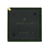
MPC561MZP56 Freescale, MPC561MZP56 Datasheet - Page 897

MPC561MZP56
Manufacturer Part Number
MPC561MZP56
Description
Manufacturer
Freescale
Datasheet
1.MPC561MZP56.pdf
(1420 pages)
Specifications of MPC561MZP56
Cpu Family
MPC56x
Device Core
PowerPC
Device Core Size
32b
Frequency (max)
56MHz
Interface Type
QSPI/SCI/SPI/UART
Total Internal Ram Size
32KB
# I/os (max)
56
Number Of Timers - General Purpose
22
Operating Supply Voltage (typ)
2.6/5V
Operating Supply Voltage (max)
2.7/5.25V
Operating Supply Voltage (min)
2.5/4.75V
On-chip Adc
2(32-chx10-bit)
Instruction Set Architecture
RISC
Operating Temp Range
-40C to 125C
Operating Temperature Classification
Automotive
Mounting
Surface Mount
Pin Count
388
Package Type
BGA
Program Memory Type
ROMLess
Program Memory Size
Not Required
Lead Free Status / RoHS Status
Not Compliant
Available stocks
Company
Part Number
Manufacturer
Quantity
Price
Company:
Part Number:
MPC561MZP56
Manufacturer:
Freescale Semiconductor
Quantity:
10 000
Company:
Part Number:
MPC561MZP56R2
Manufacturer:
Freescale Semiconductor
Quantity:
10 000
- Current page: 897 of 1420
- Download datasheet (11Mb)
Chapter 22
CALRAM Operation
The calibration static random access memory (CALRAM) module provides the MPC561/MPC563 with a
general purpose memory that may be read from or written to as either bytes, half-words, or words. In
addition to this, a portion of the CALRAM, called the overlay region, can be used for calibration.
Calibration in this context is defined as overlaying portions of the U-bus Flash with a portion of the
CALRAM array. During normal Flash access, the RISC central processing unit (RPCU) reads data from
U-bus Flash (through L-bus and L2U) as shown in
providing the data, the overlay regions of CALRAM provide the data to the RPCU.
22.1
Standard CALRAM features are listed below:
Special overlay features are:
Freescale Semiconductor
•
•
•
•
•
•
•
•
•
•
One-clock accesses
— Two-cycle access for power savings
Byte, half-word (16-bits), or word (32-bit) read/write accesses
Each 8-Kbyte block has individual protection control bits.
Low power standby operation for data retention
Eight overlay regions; each can be programmed to be 4-, 16-, 32-, 64-, 128-, 256-, or 512-bytes
long
Each overlay region size can be forced to 4 bytes long
Data driven from the CALRAM module for overlay access has the same timing as the data that
would have come from the U-bus Flash
Overlay is for data read from the U-bus Flash space and does not affect instruction fetches from
the Flash
Overlay block is naturally aligned
— For example, 128-byte block is 128-byte aligned
Normal access to overlaid portion of CALRAM array can be made to generate an error (machine
check) if so configured
Features
MPC561/MPC563 Reference Manual, Rev. 1.2
Figure
22-1. During calibration access, instead of Flash
22-1
Related parts for MPC561MZP56
Image
Part Number
Description
Manufacturer
Datasheet
Request
R

Part Number:
Description:
MPC5 1K0 5%
Manufacturer:
TE Connectivity
Datasheet:

Part Number:
Description:
MPC5 500R 5%
Manufacturer:
TE Connectivity
Datasheet:

Part Number:
Description:
MPC5 5K0 5%
Manufacturer:
Tyco Electronics
Datasheet:

Part Number:
Description:
MPC5 5R0 5%
Manufacturer:
Tyco Electronics
Datasheet:

Part Number:
Description:
MPC5 50K 5%
Manufacturer:
Tyco Electronics
Datasheet:

Part Number:
Description:
MPC5 1R0 5%
Manufacturer:
Tyco Electronics
Datasheet:

Part Number:
Description:
TOWER ELEVATOR BOARDS HARDWARE
Manufacturer:
Freescale Semiconductor
Datasheet:

Part Number:
Description:
TOWER SERIAL I/O HARDWARE
Manufacturer:
Freescale Semiconductor
Datasheet:

Part Number:
Description:
LCD MODULE FOR TWR SYSTEM
Manufacturer:
Freescale Semiconductor
Datasheet:

Part Number:
Description:
DAUGHTER LCD WVGA I.MX51
Manufacturer:
Freescale Semiconductor
Datasheet:

Part Number:
Description:
TOWER SYSTEM BOARD MPC5125
Manufacturer:
Freescale Semiconductor
Datasheet:


