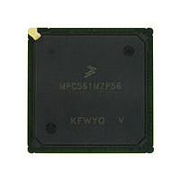
MPC561MZP56 Freescale, MPC561MZP56 Datasheet - Page 908

MPC561MZP56
Manufacturer Part Number
MPC561MZP56
Description
Manufacturer
Freescale
Datasheet
1.MPC561MZP56.pdf
(1420 pages)
Specifications of MPC561MZP56
Cpu Family
MPC56x
Device Core
PowerPC
Device Core Size
32b
Frequency (max)
56MHz
Interface Type
QSPI/SCI/SPI/UART
Total Internal Ram Size
32KB
# I/os (max)
56
Number Of Timers - General Purpose
22
Operating Supply Voltage (typ)
2.6/5V
Operating Supply Voltage (max)
2.7/5.25V
Operating Supply Voltage (min)
2.5/4.75V
On-chip Adc
2(32-chx10-bit)
Instruction Set Architecture
RISC
Operating Temp Range
-40C to 125C
Operating Temperature Classification
Automotive
Mounting
Surface Mount
Pin Count
388
Package Type
BGA
Program Memory Type
ROMLess
Program Memory Size
Not Required
Lead Free Status / RoHS Status
Not Compliant
Available stocks
Company
Part Number
Manufacturer
Quantity
Price
Company:
Part Number:
MPC561MZP56
Manufacturer:
Freescale Semiconductor
Quantity:
10 000
Company:
Part Number:
MPC561MZP56R2
Manufacturer:
Freescale Semiconductor
Quantity:
10 000
- Current page: 908 of 1420
- Download datasheet (11Mb)
CALRAM Operation
22.4.6.3
If overlay is enabled and CRAMOVLCR[DERR] is set, then any normal L-bus array access that falls
within any of the eight enabled overlay regions generates a machine-check exception; otherwise the access
terminates normally without asserting data error. The L-bus write accesses cause the data to be written
regardless of whether the DERR bit is set or not.
For example, if overlay region 1 is programmed such that it is enabled and its region size is 256 bytes, then
any L-bus access to address in the range of 0x3F F200 – 0x3F F2FF generates machine check exception
if the DERR bit is set in CRAMOVLCR register. The other portion of region 1 from 0x3F F300 to 0x3F
F3FF can be used as normal (non-overlay) array.
22.4.6.4
Write accesses to the overlaid U-bus Flash regions are ignored completely by the CALRAM module.
22.5
The following section describes the CALRAM programmer’s model. The CALRAM has one register
(CRAMMCR) for configuring the CALRAM array and one register dedicated to factory test. In addition,
there are eight 32-bit region base address registers for calibration purposes and a 32-bit overlay
configuration register. The region base address registers hold the base address for the Flash region and
region size that need to be overlaid by the CALRAM. The overlay configuration register provides three
bits (OVL, DERR, and CLSP) that are needed for overlay configuration. The CALRAM ownership trace
register (CRAM_OTR) is provided to support a separate module called a READI module. Access to all
CALRAM registers requires the bus master to be in supervisor data mode. On a privilege violation, the
register is not accessed and the access generates an error.
Table 22-2
22-12
minimal amount of reprogramming efforts.
Programming Model
shows the register address map for the MPC561/MPC563.
Normal (Non-Overlay) Access to Overlay Regions
Calibration Write Cycle Flow
Module/Region Number
CALRAM/region 0
CALRAM/region 1
CALRAM/region 2
CALRAM/region 3
CALRAM/region 4
CALRAM/region 5
CALRAM/region 6
CALRAM/region 7
Table 22-1. Priorities of Overlay Regions
MPC561/MPC563 Reference Manual, Rev. 1.2
Priority
Highest
Lowest
.
.
.
.
.
.
Freescale Semiconductor
Related parts for MPC561MZP56
Image
Part Number
Description
Manufacturer
Datasheet
Request
R

Part Number:
Description:
MPC5 1K0 5%
Manufacturer:
TE Connectivity
Datasheet:

Part Number:
Description:
MPC5 500R 5%
Manufacturer:
TE Connectivity
Datasheet:

Part Number:
Description:
MPC5 5K0 5%
Manufacturer:
Tyco Electronics
Datasheet:

Part Number:
Description:
MPC5 5R0 5%
Manufacturer:
Tyco Electronics
Datasheet:

Part Number:
Description:
MPC5 50K 5%
Manufacturer:
Tyco Electronics
Datasheet:

Part Number:
Description:
MPC5 1R0 5%
Manufacturer:
Tyco Electronics
Datasheet:

Part Number:
Description:
TOWER ELEVATOR BOARDS HARDWARE
Manufacturer:
Freescale Semiconductor
Datasheet:

Part Number:
Description:
TOWER SERIAL I/O HARDWARE
Manufacturer:
Freescale Semiconductor
Datasheet:

Part Number:
Description:
LCD MODULE FOR TWR SYSTEM
Manufacturer:
Freescale Semiconductor
Datasheet:

Part Number:
Description:
DAUGHTER LCD WVGA I.MX51
Manufacturer:
Freescale Semiconductor
Datasheet:

Part Number:
Description:
TOWER SYSTEM BOARD MPC5125
Manufacturer:
Freescale Semiconductor
Datasheet:


