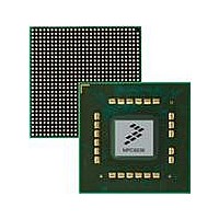
MPC8536DS Freescale Semiconductor, MPC8536DS Datasheet - Page 1045

MPC8536DS
Manufacturer Part Number
MPC8536DS
Description
BOARD DEV SYSTEM MPC8536E
Manufacturer
Freescale Semiconductor
Series
PowerQUICC III™r
Type
MPUr
Datasheets
1.MPC8536EBVTAVLA.pdf
(127 pages)
2.MPC8536EBVTAVLA.pdf
(1706 pages)
3.MPC8536DS.pdf
(2 pages)
4.MPC8536DS.pdf
(126 pages)
Specifications of MPC8536DS
Contents
Board, Software and Documentation
Processor Series
MPC85xx
Core
e500
Data Bus Width
32 bit
Maximum Clock Frequency
667 MHz
Operating Supply Voltage
- 0.3 V to + 1.21 V
Maximum Operating Temperature
+ 105 C
Data Ram Size
32 KB
Interface Type
SPI, USB
Program Memory Type
DDR2, DDR3, SDRAM
Core Size
32 Bit
Program Memory Size
544KB
Cpu Speed
1.5GHz
Digital Ic Case Style
BGA
No. Of Pins
783
Supply Voltage Range
0.95V To 1.05V
Rohs Compliant
Yes
For Use With/related Products
MPC8536
Lead Free Status / RoHS Status
Lead free / RoHS Compliant
- MPC8536EBVTAVLA PDF datasheet
- MPC8536EBVTAVLA PDF datasheet #2
- MPC8536DS PDF datasheet #3
- MPC8536DS PDF datasheet #4
- Current page: 1045 of 1706
- Download datasheet (15Mb)
16.3.1.3
The inbound address translation and mapping unit controls the mapping of transactions from the external
PCI address space to the internal platform address space. The inbound ATMU is comprised of four
windows—a configuration window and three general translation windows. The configuration window has
higher priority than all other inbound ATMU windows and takes precedence over them if there is an
overlap.
Each window contains the following:
Each window’s base address and translation address must be aligned to the size of the window. If two
general inbound ATMU windows overlap in the external PCI address space, the mappings of the lower
numbered window are applied; PCSRBAR takes priority over any overlapping inbound ATMU window.
In addition, if inbound ATMU windows are overlapped, the ATMU windows must not map to the same
address with different sets of attributes (other than window size).
Note that PCSRBAR in the PCI configuration header acts as a fourth inbound window that translates a
1-Mbyte region of PCI space to the local configuration space pointed to by CCSRBAR. PCSRBAR can
be accessed by PCI configuration cycles or by accessing the PCI configuration header through the PCI
CFG_ADDR and PCI CFG_DATA registers. See
(CFG_ADDR),” Section 16.3.1.1.2, “PCI Configuration Data Register (CFG_DATA),”
Freescale Semiconductor
•
•
•
20–25
26–31
Bits
A base address, which points to the beginning of the window in the external PCI address map. The
base address of each window is also accessible by PCI configuration transactions as base address
registers within the PCI configuration header, as shown in
or updated equivalently through the ATMU memory map or through PCI configuration
transactions to the PCI configuration header.
A translation address, which specifies the upper order bits of the transaction in the local address
space.
A set of attributes including window size and internal transaction attributes.
Name
OWS
—
PCI ATMU Inbound Registers
Reserved
Outbound window size. Outbound translation window size N which is the encoded 2^(N+1) bytes
window size. The smallest window size is 4 Kbytes.
000000Reserved
...
0010114-Kbyte window size
0011008-Kbyte window size
...
0111114-Gbyte window size
1000008-Gbyte window size
10000116-Gbyte window size
100010Reserved
...
111111Reserved
The default POWAR register (0xC10) has an OWS value of 011111.
MPC8536E PowerQUICC III Integrated Processor Reference Manual, Rev. 1
Table 16-10. POWAR n Field Descriptions (continued)
Section 16.3.1.1.1, “PCI Configuration Address Register
Description
Figure
16-26. The registers may be read
and
PCI Bus Interface
16-19
Related parts for MPC8536DS
Image
Part Number
Description
Manufacturer
Datasheet
Request
R
Part Number:
Description:
Manufacturer:
Freescale Semiconductor, Inc
Datasheet:
Part Number:
Description:
Manufacturer:
Freescale Semiconductor, Inc
Datasheet:
Part Number:
Description:
Manufacturer:
Freescale Semiconductor, Inc
Datasheet:
Part Number:
Description:
Manufacturer:
Freescale Semiconductor, Inc
Datasheet:
Part Number:
Description:
Manufacturer:
Freescale Semiconductor, Inc
Datasheet:
Part Number:
Description:
Manufacturer:
Freescale Semiconductor, Inc
Datasheet:
Part Number:
Description:
Manufacturer:
Freescale Semiconductor, Inc
Datasheet:
Part Number:
Description:
Manufacturer:
Freescale Semiconductor, Inc
Datasheet:
Part Number:
Description:
Manufacturer:
Freescale Semiconductor, Inc
Datasheet:
Part Number:
Description:
Manufacturer:
Freescale Semiconductor, Inc
Datasheet:
Part Number:
Description:
Manufacturer:
Freescale Semiconductor, Inc
Datasheet:
Part Number:
Description:
Manufacturer:
Freescale Semiconductor, Inc
Datasheet:
Part Number:
Description:
Manufacturer:
Freescale Semiconductor, Inc
Datasheet:
Part Number:
Description:
Manufacturer:
Freescale Semiconductor, Inc
Datasheet:
Part Number:
Description:
Manufacturer:
Freescale Semiconductor, Inc
Datasheet:


