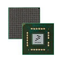
MPC8536DS Freescale Semiconductor, MPC8536DS Datasheet - Page 608

MPC8536DS
Manufacturer Part Number
MPC8536DS
Description
BOARD DEV SYSTEM MPC8536E
Manufacturer
Freescale Semiconductor
Series
PowerQUICC III™r
Type
MPUr
Datasheets
1.MPC8536EBVTAVLA.pdf
(127 pages)
2.MPC8536EBVTAVLA.pdf
(1706 pages)
3.MPC8536DS.pdf
(2 pages)
4.MPC8536DS.pdf
(126 pages)
Specifications of MPC8536DS
Contents
Board, Software and Documentation
Processor Series
MPC85xx
Core
e500
Data Bus Width
32 bit
Maximum Clock Frequency
667 MHz
Operating Supply Voltage
- 0.3 V to + 1.21 V
Maximum Operating Temperature
+ 105 C
Data Ram Size
32 KB
Interface Type
SPI, USB
Program Memory Type
DDR2, DDR3, SDRAM
Core Size
32 Bit
Program Memory Size
544KB
Cpu Speed
1.5GHz
Digital Ic Case Style
BGA
No. Of Pins
783
Supply Voltage Range
0.95V To 1.05V
Rohs Compliant
Yes
For Use With/related Products
MPC8536
Lead Free Status / RoHS Status
Lead free / RoHS Compliant
- MPC8536EBVTAVLA PDF datasheet
- MPC8536EBVTAVLA PDF datasheet #2
- MPC8536DS PDF datasheet #3
- MPC8536DS PDF datasheet #4
- Current page: 608 of 1706
- Download datasheet (15Mb)
I
11.4.3
The clock synchronization mechanism can be used as a handshake in data transfer. Slave devices can hold
SCL low after completion of a 1-byte transfer (9 bits). In such cases, it halts the bus clock and forces the
master clock into wait states until the slave releases the SCL line.
11.4.4
The clock control block handles requests from the clock signal for transferring and controlling data for
multiple tasks.
A 9-cycle data transfer clock is requested for the following conditions:
11.4.4.1
Due to the wire AND logic on the SCL line, a high-to-low transition on the SCL line affects all devices
connected on the bus. The devices begin counting their low period when the master drives the SCL line
low. After a device has driven SCL low, it holds the SCL line low until the clock high state is reached.
However, the change of low-to-high in a device clock may not change the state of the SCL line if another
device is still within its low period. Therefore, the synchronized clock signal, SCL, is held low by the
device with the longest low period. Devices with shorter low periods enter a high wait state during this
time. When all devices concerned have counted off their low period, the synchronized SCL line is released
and pulled high. Then there is no difference between the devices’ clocks and the state of the SCL line, and
all the devices begin counting their high periods. The first device to complete its high period pulls the SCL
line low again.
11.4.4.2
The following sections describes the synchronizing of the input signals, and the filtering of the SCL and
SDA lines in detail.
11.4.4.2.1
The input synchronization block synchronizes the input SCL and SDA signals to the system clock and
detects transitions of these signals.
11-16
2
C Interfaces
•
•
Master mode
— Transmit slave address after START condition
— Transmit slave address after restart condition
— Transmit data
— Receive data
Slave mode
— Transmit data
— Receive data
— Receive slave address after START or restart condition
Handshaking
Clock Control
Clock Synchronization
Input Synchronization and Digital Filter
Input Signal Synchronization
MPC8536E PowerQUICC III Integrated Processor Reference Manual, Rev. 1
Freescale Semiconductor
Related parts for MPC8536DS
Image
Part Number
Description
Manufacturer
Datasheet
Request
R
Part Number:
Description:
Manufacturer:
Freescale Semiconductor, Inc
Datasheet:
Part Number:
Description:
Manufacturer:
Freescale Semiconductor, Inc
Datasheet:
Part Number:
Description:
Manufacturer:
Freescale Semiconductor, Inc
Datasheet:
Part Number:
Description:
Manufacturer:
Freescale Semiconductor, Inc
Datasheet:
Part Number:
Description:
Manufacturer:
Freescale Semiconductor, Inc
Datasheet:
Part Number:
Description:
Manufacturer:
Freescale Semiconductor, Inc
Datasheet:
Part Number:
Description:
Manufacturer:
Freescale Semiconductor, Inc
Datasheet:
Part Number:
Description:
Manufacturer:
Freescale Semiconductor, Inc
Datasheet:
Part Number:
Description:
Manufacturer:
Freescale Semiconductor, Inc
Datasheet:
Part Number:
Description:
Manufacturer:
Freescale Semiconductor, Inc
Datasheet:
Part Number:
Description:
Manufacturer:
Freescale Semiconductor, Inc
Datasheet:
Part Number:
Description:
Manufacturer:
Freescale Semiconductor, Inc
Datasheet:
Part Number:
Description:
Manufacturer:
Freescale Semiconductor, Inc
Datasheet:
Part Number:
Description:
Manufacturer:
Freescale Semiconductor, Inc
Datasheet:
Part Number:
Description:
Manufacturer:
Freescale Semiconductor, Inc
Datasheet:


