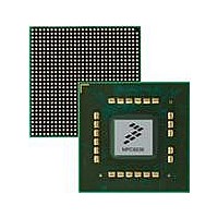
MPC8536DS Freescale Semiconductor, MPC8536DS Datasheet - Page 1295

MPC8536DS
Manufacturer Part Number
MPC8536DS
Description
BOARD DEV SYSTEM MPC8536E
Manufacturer
Freescale Semiconductor
Series
PowerQUICC III™r
Type
MPUr
Datasheets
1.MPC8536EBVTAVLA.pdf
(127 pages)
2.MPC8536EBVTAVLA.pdf
(1706 pages)
3.MPC8536DS.pdf
(2 pages)
4.MPC8536DS.pdf
(126 pages)
Specifications of MPC8536DS
Contents
Board, Software and Documentation
Processor Series
MPC85xx
Core
e500
Data Bus Width
32 bit
Maximum Clock Frequency
667 MHz
Operating Supply Voltage
- 0.3 V to + 1.21 V
Maximum Operating Temperature
+ 105 C
Data Ram Size
32 KB
Interface Type
SPI, USB
Program Memory Type
DDR2, DDR3, SDRAM
Core Size
32 Bit
Program Memory Size
544KB
Cpu Speed
1.5GHz
Digital Ic Case Style
BGA
No. Of Pins
783
Supply Voltage Range
0.95V To 1.05V
Rohs Compliant
Yes
For Use With/related Products
MPC8536
Lead Free Status / RoHS Status
Lead free / RoHS Compliant
- MPC8536EBVTAVLA PDF datasheet
- MPC8536EBVTAVLA PDF datasheet #2
- MPC8536DS PDF datasheet #3
- MPC8536DS PDF datasheet #4
- Current page: 1295 of 1706
- Download datasheet (15Mb)
Freescale Semiconductor
SDCLKFS
DTOCV
12–15
16–23
24–27
Field
8–11
DVS
28
Reserved
Data timeout counter value. Determines the interval by which SDHC_DAT line timeouts are detected. Refer to
the data timeout error
dictate timeout generation. Timeout clock frequency is generated by dividing the base clock SDHC_CLK value
by this value. When setting this register, prevent inadvertent timeout events by clearing IRQSTATEN[DTOESEN].
0000 SDHC_CLK x 2
0001 SDHC_CLK x 2
...
1110 SDHC_CLK x 2
1111 Reserved
SDHC_CLK frequency select. This field, together with DVS, selects the frequency of SDHC_CLK pin. This bit
holds the prescaler of the base clock frequency. Only the following settings are allowed:
0x01 Base clock divided by 2
0x02 Base clock divided by 4
0x04 Base clock divided by 8
0x08 Base clock divided by 16
0x10 Base clock divided by 32
0x20 Base clock divided by 64
0x40 Base clock divided by 128
0x80 Base clock divided by 256
Multiple bits must not be set or the behavior of this prescaler is undefined.
According to the SD Physical Specification version 1.1, the maximum SD clock frequency is 50 MHz, and should
never exceed this limit. The frequency of SDHC_CLK is set by the following formula:
For example, if the base clock frequency is 96 MHz, and the target frequency is 25 MHz, then choosing the
prescaler value of 0x1 and divisor value of 0x1 yields 24 MHz, which is the nearest frequency less than or equal
to the target. Similarly, to approach a clock value of 400 KHz, the prescaler value of 0x04 and divisor value of
0xE yields the exact clock value of 400 KHz.
The reset value of this bit field is 0x80. So, if the input base clock is about 96 MHz, the default SD clock after
reset is 375 KHz.
Note: The base clock frequency equals the platform clock/2.
Divisor. Provides a more exact divisor to generate the desired SD clock frequency. The settings are as follows:
0x0
0x1
...
0xE Divide by 15
0xF Divide by 16
Reserved
Divide by 1
Divide by 2
MPC8536E PowerQUICC III Integrated Processor Reference Manual, Rev. 1
Table 20-13. SYSCTL Field Descriptions (continued)
clock frequency = (base clock) / [(SDCLKFS
13
14
27
Section 20.4.10, “Interrupt Status Register
Description
(IRQSTAT)”, for information on factors that
2)
(DVS +1)]
Enhanced Secure Digital Host Controller
Eqn. 20-1
20-21
Related parts for MPC8536DS
Image
Part Number
Description
Manufacturer
Datasheet
Request
R
Part Number:
Description:
Manufacturer:
Freescale Semiconductor, Inc
Datasheet:
Part Number:
Description:
Manufacturer:
Freescale Semiconductor, Inc
Datasheet:
Part Number:
Description:
Manufacturer:
Freescale Semiconductor, Inc
Datasheet:
Part Number:
Description:
Manufacturer:
Freescale Semiconductor, Inc
Datasheet:
Part Number:
Description:
Manufacturer:
Freescale Semiconductor, Inc
Datasheet:
Part Number:
Description:
Manufacturer:
Freescale Semiconductor, Inc
Datasheet:
Part Number:
Description:
Manufacturer:
Freescale Semiconductor, Inc
Datasheet:
Part Number:
Description:
Manufacturer:
Freescale Semiconductor, Inc
Datasheet:
Part Number:
Description:
Manufacturer:
Freescale Semiconductor, Inc
Datasheet:
Part Number:
Description:
Manufacturer:
Freescale Semiconductor, Inc
Datasheet:
Part Number:
Description:
Manufacturer:
Freescale Semiconductor, Inc
Datasheet:
Part Number:
Description:
Manufacturer:
Freescale Semiconductor, Inc
Datasheet:
Part Number:
Description:
Manufacturer:
Freescale Semiconductor, Inc
Datasheet:
Part Number:
Description:
Manufacturer:
Freescale Semiconductor, Inc
Datasheet:
Part Number:
Description:
Manufacturer:
Freescale Semiconductor, Inc
Datasheet:


