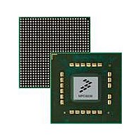
MPC8536DS Freescale Semiconductor, MPC8536DS Datasheet - Page 257

MPC8536DS
Manufacturer Part Number
MPC8536DS
Description
BOARD DEV SYSTEM MPC8536E
Manufacturer
Freescale Semiconductor
Series
PowerQUICC III™r
Type
MPUr
Datasheets
1.MPC8536EBVTAVLA.pdf
(127 pages)
2.MPC8536EBVTAVLA.pdf
(1706 pages)
3.MPC8536DS.pdf
(2 pages)
4.MPC8536DS.pdf
(126 pages)
Specifications of MPC8536DS
Contents
Board, Software and Documentation
Processor Series
MPC85xx
Core
e500
Data Bus Width
32 bit
Maximum Clock Frequency
667 MHz
Operating Supply Voltage
- 0.3 V to + 1.21 V
Maximum Operating Temperature
+ 105 C
Data Ram Size
32 KB
Interface Type
SPI, USB
Program Memory Type
DDR2, DDR3, SDRAM
Core Size
32 Bit
Program Memory Size
544KB
Cpu Speed
1.5GHz
Digital Ic Case Style
BGA
No. Of Pins
783
Supply Voltage Range
0.95V To 1.05V
Rohs Compliant
Yes
For Use With/related Products
MPC8536
Lead Free Status / RoHS Status
Lead free / RoHS Compliant
- MPC8536EBVTAVLA PDF datasheet
- MPC8536EBVTAVLA PDF datasheet #2
- MPC8536DS PDF datasheet #3
- MPC8536DS PDF datasheet #4
- Current page: 257 of 1706
- Download datasheet (15Mb)
Freescale Semiconductor
dcbtls_L2
dcbtstls_L2
Write-through store
Cache-inhibited store
Cache-inhibited stwcx
dcblc_L2
icblc_L2
Victim castout
dcbt_L2
icbt_L2
dcbtst_L2
Snoop push
dcbtls_L2
icbtls_L2
dcbtstls_L2
dcbf
dcbst
dcbz
dcba
dcbi
Source of Transaction
Table 6-27. State Transitions Due to Core-Initiated Transactions (continued)
MPC8536E PowerQUICC III Integrated Processor Reference Manual, Rev. 1
I,E,M
I,E,M
I,E,M
Initial States
dL1
dL1
N/A
N/A
dL1
dL1
dL1
dL1
dL1
dL1
I,E
L1
M
M
M
I
E/EL/T
E/EL/T
I/E/EL
E/EL
E/EL
E/EL
EL/T
EL/T
EL
I/E
I/E
I/E
EL
I/E
EL
L2
I/T
I/T
T
E
T
T
T
I/
I
I
I
I
No
Yes
Yes
Yes
Yes
Yes
Yes
Yes
Hit
No
No
No
No
No
No
No
No
No
No
No
No
No
No
No
No
No
No
No
L2
same
same
same
same
same
Final States
N/A
N/A
N/A
N/A
L1
M
M
I
I
I
I
I
I
I
I
I
I
I
I
I
I
I
I
Same L2CTL[L2IO] = 0.
same Read-modify-write
same
same L2CTL[L2IO] = 1. If software sharing cache lines
EL
EL
EL
EL
EL
EL
L2
I/T
E
T
T
T
T
E
T
I
I
I
I
I
I
I
I
I
L2CTL[L2IO] = 1
L2CTL[L2IO] = 1
L2CTL[L2IO] = 1
L2CTL[L2IO] = 1
L2CTL[L2IO] = 0
L2CTL[L2IO] = 0
L2CTL[L2IO] = 0. Restore locked line with valid
data from bus
Invalidate line
Invalidate data, keep lock
Invalidate line
Invalidate data, keep lock
between instructions and data wishes to capture
instruction lines in L2 with L2CTL[L2IO] = 1, it must
perform dcbst to flush the line out of the dL1 before
fetching it into L2.
L2CTL[L2IO] = 0
L2CTL[L2IO] = 1.
L2CTL[L2IO = 0.
An icbtls_L2 that hits modified in L1 cannot be
distinguished from dcbtls_L2 and sets the L2 dlock
bit. If software shares cache lines between
instructions and data and wishes to set hillocks in
L2, it must perform dcbst to flush the line out of the
dL1 before locking it in L2.
Comments
L2 Look-Aside Cache/SRAM
6-37
Related parts for MPC8536DS
Image
Part Number
Description
Manufacturer
Datasheet
Request
R
Part Number:
Description:
Manufacturer:
Freescale Semiconductor, Inc
Datasheet:
Part Number:
Description:
Manufacturer:
Freescale Semiconductor, Inc
Datasheet:
Part Number:
Description:
Manufacturer:
Freescale Semiconductor, Inc
Datasheet:
Part Number:
Description:
Manufacturer:
Freescale Semiconductor, Inc
Datasheet:
Part Number:
Description:
Manufacturer:
Freescale Semiconductor, Inc
Datasheet:
Part Number:
Description:
Manufacturer:
Freescale Semiconductor, Inc
Datasheet:
Part Number:
Description:
Manufacturer:
Freescale Semiconductor, Inc
Datasheet:
Part Number:
Description:
Manufacturer:
Freescale Semiconductor, Inc
Datasheet:
Part Number:
Description:
Manufacturer:
Freescale Semiconductor, Inc
Datasheet:
Part Number:
Description:
Manufacturer:
Freescale Semiconductor, Inc
Datasheet:
Part Number:
Description:
Manufacturer:
Freescale Semiconductor, Inc
Datasheet:
Part Number:
Description:
Manufacturer:
Freescale Semiconductor, Inc
Datasheet:
Part Number:
Description:
Manufacturer:
Freescale Semiconductor, Inc
Datasheet:
Part Number:
Description:
Manufacturer:
Freescale Semiconductor, Inc
Datasheet:
Part Number:
Description:
Manufacturer:
Freescale Semiconductor, Inc
Datasheet:


