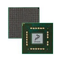
MPC8536DS Freescale Semiconductor, MPC8536DS Datasheet - Page 611

MPC8536DS
Manufacturer Part Number
MPC8536DS
Description
BOARD DEV SYSTEM MPC8536E
Manufacturer
Freescale Semiconductor
Series
PowerQUICC III™r
Type
MPUr
Datasheets
1.MPC8536EBVTAVLA.pdf
(127 pages)
2.MPC8536EBVTAVLA.pdf
(1706 pages)
3.MPC8536DS.pdf
(2 pages)
4.MPC8536DS.pdf
(126 pages)
Specifications of MPC8536DS
Contents
Board, Software and Documentation
Processor Series
MPC85xx
Core
e500
Data Bus Width
32 bit
Maximum Clock Frequency
667 MHz
Operating Supply Voltage
- 0.3 V to + 1.21 V
Maximum Operating Temperature
+ 105 C
Data Ram Size
32 KB
Interface Type
SPI, USB
Program Memory Type
DDR2, DDR3, SDRAM
Core Size
32 Bit
Program Memory Size
544KB
Cpu Speed
1.5GHz
Digital Ic Case Style
BGA
No. Of Pins
783
Supply Voltage Range
0.95V To 1.05V
Rohs Compliant
Yes
For Use With/related Products
MPC8536
Lead Free Status / RoHS Status
Lead free / RoHS Compliant
- MPC8536EBVTAVLA PDF datasheet
- MPC8536EBVTAVLA PDF datasheet #2
- MPC8536DS PDF datasheet #3
- MPC8536DS PDF datasheet #4
- Current page: 611 of 1706
- Download datasheet (15Mb)
11.4.5.2
The I
be the first 3 bytes programmed into the EEPROM. It should have a value of 0xAA55AA. The I
checks to ensure that this preamble is correctly detected before proceeding further. Following the
preamble, there should be a series of configuration registers (known as register preloads) programmed into
the EEPROM. Each configuration register should be programmed according to a particular format, as
shown in
contained are alternate configuration space (ACS), byte enables, and continue (CONT). The boot
sequencer expects the address offset to be a 32-bit (word) offset, that is, the 2 low-order bits are not
included in the boot sequencer command. For example, to access LAWBAR0 (byte offset of 0x00C08),
the boot sequencer ADDR[0:17] should be set to 0x00302.
After the first 3 bytes, 4 bytes of data should hold the desired value of the configuration register, regardless
of the size of the transaction. Byte enables should be asserted for any byte that is written to the
configuration register, and they should be asserted contiguously, creating a 1-, 2-, or 4-byte write to a
register. The boot sequencer assumes that a big-endian address is stored in the EEPROM. In addition, byte
enable bit 0 (bit 1 of the byte) corresponds to the most-significant byte of data (data[0:7]), and byte enable
bit 3 (bit 4 of the byte) corresponds to the LSB of data (data[24:31]).
By setting ACS, an alternate configuration space address is prepended to the write request from the boot
sequencer. Otherwise, CCSRBAR is prepended to the EEPROM address.
If CONT is cleared, the first 3 bytes, including ACS, the byte enables, and the address, must also be
cleared. Also, the data contains the final cyclic redundancy check (CRC). A CRC-32 algorithm is used to
check the integrity of the data. The polynomial used is:
CRC values are calculated using the above polynomial with a start value of 0xFFFF_FFFF and an XOR
with 0x0000_0000. The CRC should cover all bytes stored in the EEPROM prior to the CRC. This
includes the preamble, all register preloads, and the first 3 bytes of the last 7-byte preload (which should
be all zeros). If a preamble or CRC fail is detected, the device hangs and the external HRESET_REQ signal
asserts. If there is a preamble fail, the boot sequencer may continue to pull I
occurs.
Freescale Semiconductor
2
C module expects that a particular data format be used for data in the EEPROM. A preamble should
Figure
1 + x
EEPROM Data Format
1
11-9. The first 3 bytes hold the attributes and address offset, as follows. The attributes
Figure 11-9. EEPROM Data Format for One Register Preload Command
+ x
MPC8536E PowerQUICC III Integrated Processor Reference Manual, Rev. 1
2
+ x
4
+ x
ACS
5
0
+ x
7
+ x
1
8
BYTE_EN
+ x
10
ADDR[10–17]
DATA[16–23]
DATA[24–31]
ADDR[2–9]
DATA[8–15]
DATA[0–7]
+ x
11
4
+ x
12
CONT ADDR[0–1]
5
+ x
16
+ x
6
22
7
+ x
23
2
C pins low until a hard reset
+ x
26
+ x
32
2
I
2
C module
C Interfaces
11-19
Related parts for MPC8536DS
Image
Part Number
Description
Manufacturer
Datasheet
Request
R
Part Number:
Description:
Manufacturer:
Freescale Semiconductor, Inc
Datasheet:
Part Number:
Description:
Manufacturer:
Freescale Semiconductor, Inc
Datasheet:
Part Number:
Description:
Manufacturer:
Freescale Semiconductor, Inc
Datasheet:
Part Number:
Description:
Manufacturer:
Freescale Semiconductor, Inc
Datasheet:
Part Number:
Description:
Manufacturer:
Freescale Semiconductor, Inc
Datasheet:
Part Number:
Description:
Manufacturer:
Freescale Semiconductor, Inc
Datasheet:
Part Number:
Description:
Manufacturer:
Freescale Semiconductor, Inc
Datasheet:
Part Number:
Description:
Manufacturer:
Freescale Semiconductor, Inc
Datasheet:
Part Number:
Description:
Manufacturer:
Freescale Semiconductor, Inc
Datasheet:
Part Number:
Description:
Manufacturer:
Freescale Semiconductor, Inc
Datasheet:
Part Number:
Description:
Manufacturer:
Freescale Semiconductor, Inc
Datasheet:
Part Number:
Description:
Manufacturer:
Freescale Semiconductor, Inc
Datasheet:
Part Number:
Description:
Manufacturer:
Freescale Semiconductor, Inc
Datasheet:
Part Number:
Description:
Manufacturer:
Freescale Semiconductor, Inc
Datasheet:
Part Number:
Description:
Manufacturer:
Freescale Semiconductor, Inc
Datasheet:


