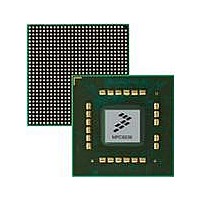
MPC8536DS Freescale Semiconductor, MPC8536DS Datasheet - Page 177

MPC8536DS
Manufacturer Part Number
MPC8536DS
Description
BOARD DEV SYSTEM MPC8536E
Manufacturer
Freescale Semiconductor
Series
PowerQUICC III™r
Type
MPUr
Datasheets
1.MPC8536EBVTAVLA.pdf
(127 pages)
2.MPC8536EBVTAVLA.pdf
(1706 pages)
3.MPC8536DS.pdf
(2 pages)
4.MPC8536DS.pdf
(126 pages)
Specifications of MPC8536DS
Contents
Board, Software and Documentation
Processor Series
MPC85xx
Core
e500
Data Bus Width
32 bit
Maximum Clock Frequency
667 MHz
Operating Supply Voltage
- 0.3 V to + 1.21 V
Maximum Operating Temperature
+ 105 C
Data Ram Size
32 KB
Interface Type
SPI, USB
Program Memory Type
DDR2, DDR3, SDRAM
Core Size
32 Bit
Program Memory Size
544KB
Cpu Speed
1.5GHz
Digital Ic Case Style
BGA
No. Of Pins
783
Supply Voltage Range
0.95V To 1.05V
Rohs Compliant
Yes
For Use With/related Products
MPC8536
Lead Free Status / RoHS Status
Lead free / RoHS Compliant
- MPC8536EBVTAVLA PDF datasheet
- MPC8536EBVTAVLA PDF datasheet #2
- MPC8536DS PDF datasheet #3
- MPC8536DS PDF datasheet #4
- Current page: 177 of 1706
- Download datasheet (15Mb)
4.3.1.3
When the e500 core comes out of reset, its MMU has one 4-Kbyte page defined at 0x0_FFFF_Fnnn. The
core begins execution with the instruction at effective address 0x0_FFFF_FFFC. To get this instruction,
the core’s first instruction fetch is a burst read of boot code from effective address 0x0_FFFF_FFE0. For
systems in which the boot code resides at a different address, the MPC8536E provides boot page
translation capability. Boot page translation is controlled by the boot page translation register (BPTR).
The boot sequencer can enable boot page translation, or the boot page translation can be set up by an
external host when the device is configured to be in boot holdoff mode. If translation is to be performed to
a page outside the default boot ROM address range defined in the MPC8536E (8 Mbytes at
0x0_FF80_0000 to 0x0_FFFF_FFFF as defined in
host or boot sequencer must then also set up a local access window to define the routing of the boot code
fetch to the target interface that contains the boot code, because the BPTR defines only the address
translation, not the target interface. See
Section 11.4.5, “Boot Sequencer Mode,”
4.3.1.3.1
Figure 4-4
Freescale Semiconductor
12–31
7–11
Bits
Offset 0x0_0020
Reset
W
R
TRGT_ID
EN
0
Name
shows the fields of BPTR.
—
1
Boot Page Translation
Boot Page Translation Register (BPTR)
second configuration window.
00000 PCI Interface
00001 PCI Express 2
00010 PCI Express 1
00011 PCI Express 3
00100 Local bus controller
Write reserved, read = 0
Identifies the device ID to target when a transaction hits in the 1-Mbyte address range defined by the
MPC8536E PowerQUICC III Integrated Processor Reference Manual, Rev. 1
—
Figure 4-4. Boot Page Translation Register (BPTR)
Table 4-7. ALTCAR Bit Settings (continued)
7
8
Section 2.1, “Local Memory Map Overview and Example,”
for more information.
Section 4.4.3.6, “Boot ROM
All zeros
00101–01011 Reserved
01000 Configuration, control, status registers
01001–01110 Reserved
01111 Local memory—DDR SDRAM and on-chip SRAM
Description
BOOT_PAGE
Reset, Clocking, and Initialization
Location”), the external
Access: Read/Write
and
4-7
31
Related parts for MPC8536DS
Image
Part Number
Description
Manufacturer
Datasheet
Request
R
Part Number:
Description:
Manufacturer:
Freescale Semiconductor, Inc
Datasheet:
Part Number:
Description:
Manufacturer:
Freescale Semiconductor, Inc
Datasheet:
Part Number:
Description:
Manufacturer:
Freescale Semiconductor, Inc
Datasheet:
Part Number:
Description:
Manufacturer:
Freescale Semiconductor, Inc
Datasheet:
Part Number:
Description:
Manufacturer:
Freescale Semiconductor, Inc
Datasheet:
Part Number:
Description:
Manufacturer:
Freescale Semiconductor, Inc
Datasheet:
Part Number:
Description:
Manufacturer:
Freescale Semiconductor, Inc
Datasheet:
Part Number:
Description:
Manufacturer:
Freescale Semiconductor, Inc
Datasheet:
Part Number:
Description:
Manufacturer:
Freescale Semiconductor, Inc
Datasheet:
Part Number:
Description:
Manufacturer:
Freescale Semiconductor, Inc
Datasheet:
Part Number:
Description:
Manufacturer:
Freescale Semiconductor, Inc
Datasheet:
Part Number:
Description:
Manufacturer:
Freescale Semiconductor, Inc
Datasheet:
Part Number:
Description:
Manufacturer:
Freescale Semiconductor, Inc
Datasheet:
Part Number:
Description:
Manufacturer:
Freescale Semiconductor, Inc
Datasheet:
Part Number:
Description:
Manufacturer:
Freescale Semiconductor, Inc
Datasheet:


