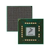
MPC8536DS Freescale Semiconductor, MPC8536DS Datasheet - Page 609

MPC8536DS
Manufacturer Part Number
MPC8536DS
Description
BOARD DEV SYSTEM MPC8536E
Manufacturer
Freescale Semiconductor
Series
PowerQUICC III™r
Type
MPUr
Datasheets
1.MPC8536EBVTAVLA.pdf
(127 pages)
2.MPC8536EBVTAVLA.pdf
(1706 pages)
3.MPC8536DS.pdf
(2 pages)
4.MPC8536DS.pdf
(126 pages)
Specifications of MPC8536DS
Contents
Board, Software and Documentation
Processor Series
MPC85xx
Core
e500
Data Bus Width
32 bit
Maximum Clock Frequency
667 MHz
Operating Supply Voltage
- 0.3 V to + 1.21 V
Maximum Operating Temperature
+ 105 C
Data Ram Size
32 KB
Interface Type
SPI, USB
Program Memory Type
DDR2, DDR3, SDRAM
Core Size
32 Bit
Program Memory Size
544KB
Cpu Speed
1.5GHz
Digital Ic Case Style
BGA
No. Of Pins
783
Supply Voltage Range
0.95V To 1.05V
Rohs Compliant
Yes
For Use With/related Products
MPC8536
Lead Free Status / RoHS Status
Lead free / RoHS Compliant
- MPC8536EBVTAVLA PDF datasheet
- MPC8536EBVTAVLA PDF datasheet #2
- MPC8536DS PDF datasheet #3
- MPC8536DS PDF datasheet #4
- Current page: 609 of 1706
- Download datasheet (15Mb)
11.4.4.2.2
The SCL and SDA inputs are filtered to eliminate noise. Three consecutive samples of the SCL and SDA
lines are compared to a pre-determined sampling rate. If they are all high, the output of the filter is high.
If they are all low, the output is low. If they are any combination of highs and lows, the output is whatever
the value of the line was in the previous clock cycle.
The sampling rate is equal to a binary value stored in the frequency register I2CDFSRR. The duration of
the sampling cycle is controlled by a down counter. This allows a software write to the frequency register
to control the filtered sampling rate.
11.4.4.3
Slaves can use the clock synchronization mechanism to slow down the transfer bit rate. After the master
has driven the SCL line low, the slave can drive SCL low for the required period and then release it. If the
slave SCL low period is greater than the master SCL low period, then the resulting SCL bus signal low
period is stretched.
11.4.5
If boot sequencer mode is selected on POR (by the settings on the cfg_boot_seq[0:1] reset configuration
signals, as described in
communicates with one or more EEPROMs through the I
boot sequencer accesses the I
(CCB) clock frequency divided by 2560. The EEPROM(s) can be programmed to initialize one or more
configuration registers of this integrated device.
If the boot sequencer is enabled for normal I
sequence during reset:
Freescale Semiconductor
1. Generate RESET sequence (START then 9 SCL cycles) to the EEPROM twice. This clears any
2. Generate START
3. Transmit 0xA0 which is the 7-bit calling address (0b101_0000) with a write command appended
4. Transmit 0x00 which is the 8-bit starting address
5. Generate a repeated START
6. Transmit 0xA1 which is the 7-bit calling address (0b101_0000) with a read command appended (1
7. Receive 256 bytes of data from the EEPROM (unless the CONT bit is cleared in the data structure).
8. Generate a repeated START
9. Transmit 0xA2 which is the 7-bit calling address of the second target (0b101_0001) with a write
10. Transmit 0x00 which is the 8-bit starting address for the second target.
11. Generate a repeated START
transactions that may have been in progress prior to the reset.
(0 as the least significant bit).
as the least significant bit).
command appended (0 as the least significant bit).
Boot Sequencer Mode
Clock Stretching
Filtering of SCL and SDA Lines
MPC8536E PowerQUICC III Integrated Processor Reference Manual, Rev. 1
Section 4.4.3.11, “Boot Sequencer
2
C1 serial ROM device at a serial bit clock frequency equal to the platform
2
C addressing mode, the I
2
C interface on IIC1_SCL and IIC1_SDA. The
Configuration”), the I
2
C interface initiates the following
2
C1 module
I
2
C Interfaces
11-17
Related parts for MPC8536DS
Image
Part Number
Description
Manufacturer
Datasheet
Request
R
Part Number:
Description:
Manufacturer:
Freescale Semiconductor, Inc
Datasheet:
Part Number:
Description:
Manufacturer:
Freescale Semiconductor, Inc
Datasheet:
Part Number:
Description:
Manufacturer:
Freescale Semiconductor, Inc
Datasheet:
Part Number:
Description:
Manufacturer:
Freescale Semiconductor, Inc
Datasheet:
Part Number:
Description:
Manufacturer:
Freescale Semiconductor, Inc
Datasheet:
Part Number:
Description:
Manufacturer:
Freescale Semiconductor, Inc
Datasheet:
Part Number:
Description:
Manufacturer:
Freescale Semiconductor, Inc
Datasheet:
Part Number:
Description:
Manufacturer:
Freescale Semiconductor, Inc
Datasheet:
Part Number:
Description:
Manufacturer:
Freescale Semiconductor, Inc
Datasheet:
Part Number:
Description:
Manufacturer:
Freescale Semiconductor, Inc
Datasheet:
Part Number:
Description:
Manufacturer:
Freescale Semiconductor, Inc
Datasheet:
Part Number:
Description:
Manufacturer:
Freescale Semiconductor, Inc
Datasheet:
Part Number:
Description:
Manufacturer:
Freescale Semiconductor, Inc
Datasheet:
Part Number:
Description:
Manufacturer:
Freescale Semiconductor, Inc
Datasheet:
Part Number:
Description:
Manufacturer:
Freescale Semiconductor, Inc
Datasheet:


