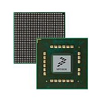
MPC8536DS Freescale Semiconductor, MPC8536DS Datasheet - Page 659

MPC8536DS
Manufacturer Part Number
MPC8536DS
Description
BOARD DEV SYSTEM MPC8536E
Manufacturer
Freescale Semiconductor
Series
PowerQUICC III™r
Type
MPUr
Datasheets
1.MPC8536EBVTAVLA.pdf
(127 pages)
2.MPC8536EBVTAVLA.pdf
(1706 pages)
3.MPC8536DS.pdf
(2 pages)
4.MPC8536DS.pdf
(126 pages)
Specifications of MPC8536DS
Contents
Board, Software and Documentation
Processor Series
MPC85xx
Core
e500
Data Bus Width
32 bit
Maximum Clock Frequency
667 MHz
Operating Supply Voltage
- 0.3 V to + 1.21 V
Maximum Operating Temperature
+ 105 C
Data Ram Size
32 KB
Interface Type
SPI, USB
Program Memory Type
DDR2, DDR3, SDRAM
Core Size
32 Bit
Program Memory Size
544KB
Cpu Speed
1.5GHz
Digital Ic Case Style
BGA
No. Of Pins
783
Supply Voltage Range
0.95V To 1.05V
Rohs Compliant
Yes
For Use With/related Products
MPC8536
Lead Free Status / RoHS Status
Lead free / RoHS Compliant
- MPC8536EBVTAVLA PDF datasheet
- MPC8536EBVTAVLA PDF datasheet #2
- MPC8536DS PDF datasheet #3
- MPC8536DS PDF datasheet #4
- Current page: 659 of 1706
- Download datasheet (15Mb)
Table 13-8
Freescale Semiconductor
17–18
0–16
Bits
19
20
21
22
23
BCTLD
Name
CSCT
PGS
CST
AM
—
—
describes ORn fields for FCM mode.
FCM address mask. Masks corresponding BR n bits. Masking address bits independently allows external
devices of different size address ranges to be used. Address mask bits can be set or cleared in any order
in the field, allowing a resource to reside in more than one area of the address map.
0 Corresponding address bits are masked.
1 Corresponding address bits are used in the comparison between base and transaction addresses.
Reserved
Buffer control disable. Disables assertion of LBCTL during access to the current memory bank.
0 LBCTL is asserted upon access to the current memory bank.
1 LBCTL is not asserted upon access to the current memory bank.
Reserved
NAND Flash EEPROM page size, buffer size, and block size.
0 Page size of 512 main area bytes plus 16 spare area bytes (small page devices);
1 Page size of 2048 main area bytes plus 64 spare area bytes (large page devices);
Chip select to command time. Determines how far in advance LCS n is asserted prior to any bus activity
during a NAND Flash access handled by the FCM. This helps meet chip-select setup times for slow
memories.
Command setup time. Determines the delay of LFWE assertion relative to the command, address, or data
change when the external memory access is handled by the FCM.
FCM RAM buffers are 1 Kbyte each; Flash block size of 16 Kbytes.
FCM RAM buffers are 4 Kbytes each; Flash block size of 128 Kbytes.
MPC8536E PowerQUICC III Integrated Processor Reference Manual, Rev. 1
TRLX
TRLX
0
0
1
1
0
0
1
1
CSCT
CST
0
1
0
1
0
1
0
1
Table 13-8. OR n
The chip-select is asserted 1 clock cycle before any command.
The chip-select is asserted 4 clock cycles before any command.
The chip-select is asserted 2 clock cycles before any command.
The chip-select is asserted 8 clock cycles before any command.
The write-enable is asserted coincident with any command.
The write-enable is asserted 0.25 clock cycles after any command, address, or
data.
The write-enable is asserted 0.5 clock cycles after any command, address, or
data.
The write-enable is asserted 1 clock cycle after any command, address, or data.
—
FCM Field Descriptions
Description
Meaning
Meaning
Enhanced Local Bus Controller
13-17
Related parts for MPC8536DS
Image
Part Number
Description
Manufacturer
Datasheet
Request
R
Part Number:
Description:
Manufacturer:
Freescale Semiconductor, Inc
Datasheet:
Part Number:
Description:
Manufacturer:
Freescale Semiconductor, Inc
Datasheet:
Part Number:
Description:
Manufacturer:
Freescale Semiconductor, Inc
Datasheet:
Part Number:
Description:
Manufacturer:
Freescale Semiconductor, Inc
Datasheet:
Part Number:
Description:
Manufacturer:
Freescale Semiconductor, Inc
Datasheet:
Part Number:
Description:
Manufacturer:
Freescale Semiconductor, Inc
Datasheet:
Part Number:
Description:
Manufacturer:
Freescale Semiconductor, Inc
Datasheet:
Part Number:
Description:
Manufacturer:
Freescale Semiconductor, Inc
Datasheet:
Part Number:
Description:
Manufacturer:
Freescale Semiconductor, Inc
Datasheet:
Part Number:
Description:
Manufacturer:
Freescale Semiconductor, Inc
Datasheet:
Part Number:
Description:
Manufacturer:
Freescale Semiconductor, Inc
Datasheet:
Part Number:
Description:
Manufacturer:
Freescale Semiconductor, Inc
Datasheet:
Part Number:
Description:
Manufacturer:
Freescale Semiconductor, Inc
Datasheet:
Part Number:
Description:
Manufacturer:
Freescale Semiconductor, Inc
Datasheet:
Part Number:
Description:
Manufacturer:
Freescale Semiconductor, Inc
Datasheet:


